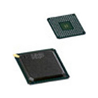
PNX1302EH NXP Semiconductors, PNX1302EH Datasheet - Page 226

PNX1302EH
Manufacturer Part Number
PNX1302EH
Description
Manufacturer
NXP Semiconductors
Datasheet
1.PNX1302EH.pdf
(548 pages)
Specifications of PNX1302EH
Lead Free Status / RoHS Status
Not Compliant
Available stocks
Company
Part Number
Manufacturer
Quantity
Price
Company:
Part Number:
PNX1302EH
Manufacturer:
NXP
Quantity:
201
Part Number:
PNX1302EH
Manufacturer:
PHILIPS/飞利浦
Quantity:
20 000
Company:
Part Number:
PNX1302EH,557
Manufacturer:
NXP Semiconductors
Quantity:
10 000
Company:
Part Number:
PNX1302EH/G
Manufacturer:
NXP
Quantity:
5 510
Part Number:
PNX1302EH/G
Manufacturer:
NXP/恩智浦
Quantity:
20 000
- Current page: 226 of 548
- Download datasheet (6Mb)
PNX1300/01/02/11 Data Book
up scaled by 2 relative to the Y component for YUV 4:4:4
output, although they could be up scaled as part of gen-
eral up scaling of the image.
The YUV 4:2:2 output mode also provides higher pro-
cessing bandwidth relative to YUV 4:4:4 up scaling. Half
as many U and V pixels are processed.The output pixel
rate is one pixel per 20 nanoseconds for the YUV 4:2:2
output mode versus one pixel per 30 for conversion to
YUV 4:4:4. This can be used to provide some processing
performance improvement for very large images at the
expense of some chroma quality.
14.5.9.2
The ICP outputs pixels to the PCI interface at a peak rate
of 33 Mpix/sec in RGB mode and 50 Mpix/second in the
14-16
Figure 14-16. ICP horizontal scaling for RGB output data flow block diagram
U LSB Counter
Y LSB Counter
V LSB Counter
B, BX Counter
Block FIFO
Block FIFO
Block FIFO
Buffers 0,1
Buffers 2,3
Buffers 4,5
Buffers 6,7
Y Counter
U Counter
V Counter
OL Counter
Bit Mask
Buffer 8
Overlay
FIFO
PCI output block timing
PRELIMINARY SPECIFICATION
Filter Source Select
Pixel
Clock
Reg
Reg
Reg
Reg
Reg
Reg
Reg
Reg
Reg
Reg
Reg
Reg
Sequence
Counter
YUV
Y Mirror Cntr
U Mirror Cntr
V Mirror Cntr
YUV mode using YUV sequencing. For one word per pix-
el output codes, such as RGB-24, this is a peak rate of
33 Mwords/sec or 132 Mpix/sec in the RGB sequencing
mode. This is the same speed as the 132 MB/sec peak
rate of the PCI interface. (At 50 Mpix/sec, the result
would be 200 MB/sec.) The BIU control for the PCI inter-
face has a FIFO for buffering data from the ICP, but this
buffer is only 16 words deep. Therefore, the ICP will oc-
casionally have to wait for the PCI to accept more data.
In the PCI output mode, this stalls the ICP clock.
14.6
The ICP uses a combination of hardware and a Micro-
program Control Unit (MCU) to implement its scaling, fil-
tering and conversion functions. The microprogram is a
Y, U, V Data FIFO Clocks
RGB to PCI case
RGB to SDRAM case
OPERATION AND PROGRAMMING
5 Stage Multiplier-
Accumulator
5-tap Filter
Y, U, V LSBs
Philips Semiconductors
Related parts for PNX1302EH
Image
Part Number
Description
Manufacturer
Datasheet
Request
R
Part Number:
Description:
NXP Semiconductors designed the LPC2420/2460 microcontroller around a 16-bit/32-bitARM7TDMI-S CPU core with real-time debug interfaces that include both JTAG andembedded trace
Manufacturer:
NXP Semiconductors
Datasheet:

Part Number:
Description:
NXP Semiconductors designed the LPC2458 microcontroller around a 16-bit/32-bitARM7TDMI-S CPU core with real-time debug interfaces that include both JTAG andembedded trace
Manufacturer:
NXP Semiconductors
Datasheet:
Part Number:
Description:
NXP Semiconductors designed the LPC2468 microcontroller around a 16-bit/32-bitARM7TDMI-S CPU core with real-time debug interfaces that include both JTAG andembedded trace
Manufacturer:
NXP Semiconductors
Datasheet:
Part Number:
Description:
NXP Semiconductors designed the LPC2470 microcontroller, powered by theARM7TDMI-S core, to be a highly integrated microcontroller for a wide range ofapplications that require advanced communications and high quality graphic displays
Manufacturer:
NXP Semiconductors
Datasheet:
Part Number:
Description:
NXP Semiconductors designed the LPC2478 microcontroller, powered by theARM7TDMI-S core, to be a highly integrated microcontroller for a wide range ofapplications that require advanced communications and high quality graphic displays
Manufacturer:
NXP Semiconductors
Datasheet:
Part Number:
Description:
The Philips Semiconductors XA (eXtended Architecture) family of 16-bit single-chip microcontrollers is powerful enough to easily handle the requirements of high performance embedded applications, yet inexpensive enough to compete in the market for hi
Manufacturer:
NXP Semiconductors
Datasheet:
Part Number:
Description:
The XA-S3 device is a member of Philips Semiconductors? XA(eXtended Architecture) family of high performance 16-bitsingle-chip microcontrollers
Manufacturer:
NXP Semiconductors
Datasheet:

Part Number:
Description:
The NXP BlueStreak LH75401/LH75411 family consists of two low-cost 16/32-bit System-on-Chip (SoC) devices
Manufacturer:
NXP Semiconductors
Datasheet:

Part Number:
Description:
The NXP LPC3130/3131 combine an 180 MHz ARM926EJ-S CPU core, high-speed USB2
Manufacturer:
NXP Semiconductors
Datasheet:

Part Number:
Description:
The NXP LPC3141 combine a 270 MHz ARM926EJ-S CPU core, High-speed USB 2
Manufacturer:
NXP Semiconductors

Part Number:
Description:
The NXP LPC3143 combine a 270 MHz ARM926EJ-S CPU core, High-speed USB 2
Manufacturer:
NXP Semiconductors

Part Number:
Description:
The NXP LPC3152 combines an 180 MHz ARM926EJ-S CPU core, High-speed USB 2
Manufacturer:
NXP Semiconductors

Part Number:
Description:
The NXP LPC3154 combines an 180 MHz ARM926EJ-S CPU core, High-speed USB 2
Manufacturer:
NXP Semiconductors

Part Number:
Description:
Standard level N-channel enhancement mode Field-Effect Transistor (FET) in a plastic package using NXP High-Performance Automotive (HPA) TrenchMOS technology
Manufacturer:
NXP Semiconductors
Datasheet:


