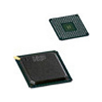
PNX1302EH NXP Semiconductors, PNX1302EH Datasheet - Page 262

PNX1302EH
Manufacturer Part Number
PNX1302EH
Description
Manufacturer
NXP Semiconductors
Datasheet
1.PNX1302EH.pdf
(548 pages)
Specifications of PNX1302EH
Lead Free Status / RoHS Status
Not Compliant
Available stocks
Company
Part Number
Manufacturer
Quantity
Price
Company:
Part Number:
PNX1302EH
Manufacturer:
NXP
Quantity:
201
Part Number:
PNX1302EH
Manufacturer:
PHILIPS/飞利浦
Quantity:
20 000
Company:
Part Number:
PNX1302EH,557
Manufacturer:
NXP Semiconductors
Quantity:
10 000
Company:
Part Number:
PNX1302EH/G
Manufacturer:
NXP
Quantity:
5 510
Part Number:
PNX1302EH/G
Manufacturer:
NXP/恩智浦
Quantity:
20 000
- Current page: 262 of 548
- Download datasheet (6Mb)
PNX1300/01/02/11 Data Book
17.9
The SSI unit has two test modes which can be controlled
by setting SSI_CSR.TMS. A remote and a local loop
back testmode are supported (see also
17.9.1
This test mode allows a remote transmitter to test itself,
the intervening transmission media, and its associated
receiver. In this mode, the data received on the
SSI_RxDATA pin is buffered and transmitted on the
SSI_TxDATA pin. The data is not transferred to
SSI_TxDR/TxFIFO and the DSPCPU is never interrupt-
ed. The transmitter is clocked by the SSI_RxCLK pin with
a combinatorial clock delay.
17.9.2
This test mode allows the DSPCPU to run local checks
of the SSI. Data written to the TxFIFO is serialized and
17-8
Figure 17-10. SSI MMIO registers.
MMIO_BASE
0x10 2C00
0x10 2C04
0x10 2C10
0x10 2C20
0x10 2C24
reset: 0x00f00000
reset: 0x0000f000
offset:
SSI TEST MODES
Local Loopback
Remote Loopback
SSI_CTL (r/w)
SSI_CSR (r/w)
SSI_TXDR (w/o)
SSI_RXDR (r/o)
SSI_RXACK (w/o)
PRELIMINARY SPECIFICATION
TXR
RXR
TMS
31
31
TXE
31
CDE
RXE
Table
TCP
CD2
RCP
SLP
TSD
17-9).
RSD
27
27
27
CTUE
23
23
23
IO1 IO2
SROE
passed to the receiver via an internal serial connection.
The receiver deserializes the data and passes it to the
RxFIFO register. Interrupts will be generated if enabled.
During local loop back mode, the data on the
SSI_RxDATA pin is ignored and the SSI_TxDATA pin is
tristated. An external CLK must be provided during local
loop back mode or no transmission or reception will oc-
cur.
17.10 MMIO REGISTERS
The MMIO Control and Status registers are shown in
Figure
Table
Table
any undefined MMIO bits should be ignored when read,
and written as ‘0’s.
CFES
WIO1
CCDS
WIO2
19
19
19
17-5,
17-9. To ensure compatibility with future devices,
TIE
17-10. The register fields are described in
RIE
TXDATA
RXDATA
Table
15
15
15
WAW
FSS
17-6,
11
11
11
Table
Philips Semiconductors
FMS
WAR
VSS
FSP
TDE
MOD
RDF
17-7,
EMS
TUE
7
ROE
7
7
FES
Table
CDS
RIO1
RIO2
RX_ACK
3
3
3
17-8, and
ILS
0
0
0
Related parts for PNX1302EH
Image
Part Number
Description
Manufacturer
Datasheet
Request
R
Part Number:
Description:
NXP Semiconductors designed the LPC2420/2460 microcontroller around a 16-bit/32-bitARM7TDMI-S CPU core with real-time debug interfaces that include both JTAG andembedded trace
Manufacturer:
NXP Semiconductors
Datasheet:

Part Number:
Description:
NXP Semiconductors designed the LPC2458 microcontroller around a 16-bit/32-bitARM7TDMI-S CPU core with real-time debug interfaces that include both JTAG andembedded trace
Manufacturer:
NXP Semiconductors
Datasheet:
Part Number:
Description:
NXP Semiconductors designed the LPC2468 microcontroller around a 16-bit/32-bitARM7TDMI-S CPU core with real-time debug interfaces that include both JTAG andembedded trace
Manufacturer:
NXP Semiconductors
Datasheet:
Part Number:
Description:
NXP Semiconductors designed the LPC2470 microcontroller, powered by theARM7TDMI-S core, to be a highly integrated microcontroller for a wide range ofapplications that require advanced communications and high quality graphic displays
Manufacturer:
NXP Semiconductors
Datasheet:
Part Number:
Description:
NXP Semiconductors designed the LPC2478 microcontroller, powered by theARM7TDMI-S core, to be a highly integrated microcontroller for a wide range ofapplications that require advanced communications and high quality graphic displays
Manufacturer:
NXP Semiconductors
Datasheet:
Part Number:
Description:
The Philips Semiconductors XA (eXtended Architecture) family of 16-bit single-chip microcontrollers is powerful enough to easily handle the requirements of high performance embedded applications, yet inexpensive enough to compete in the market for hi
Manufacturer:
NXP Semiconductors
Datasheet:
Part Number:
Description:
The XA-S3 device is a member of Philips Semiconductors? XA(eXtended Architecture) family of high performance 16-bitsingle-chip microcontrollers
Manufacturer:
NXP Semiconductors
Datasheet:

Part Number:
Description:
The NXP BlueStreak LH75401/LH75411 family consists of two low-cost 16/32-bit System-on-Chip (SoC) devices
Manufacturer:
NXP Semiconductors
Datasheet:

Part Number:
Description:
The NXP LPC3130/3131 combine an 180 MHz ARM926EJ-S CPU core, high-speed USB2
Manufacturer:
NXP Semiconductors
Datasheet:

Part Number:
Description:
The NXP LPC3141 combine a 270 MHz ARM926EJ-S CPU core, High-speed USB 2
Manufacturer:
NXP Semiconductors

Part Number:
Description:
The NXP LPC3143 combine a 270 MHz ARM926EJ-S CPU core, High-speed USB 2
Manufacturer:
NXP Semiconductors

Part Number:
Description:
The NXP LPC3152 combines an 180 MHz ARM926EJ-S CPU core, High-speed USB 2
Manufacturer:
NXP Semiconductors

Part Number:
Description:
The NXP LPC3154 combines an 180 MHz ARM926EJ-S CPU core, High-speed USB 2
Manufacturer:
NXP Semiconductors

Part Number:
Description:
Standard level N-channel enhancement mode Field-Effect Transistor (FET) in a plastic package using NXP High-Performance Automotive (HPA) TrenchMOS technology
Manufacturer:
NXP Semiconductors
Datasheet:


