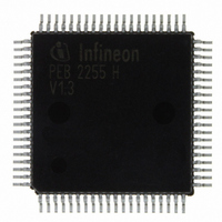
PEB2255H-V13 Infineon Technologies, PEB2255H-V13 Datasheet - Page 115

PEB2255H-V13
Manufacturer Part Number
PEB2255H-V13
Description
IC INTERFACE LINE 80-MQFP
Manufacturer
Infineon Technologies
Datasheet
1.PEB2255H-V13.pdf
(374 pages)
Specifications of PEB2255H-V13
Applications
*
Interface
*
Voltage - Supply
*
Package / Case
80-SQFP
Mounting Type
Surface Mount
Lead Free Status / RoHS Status
Lead free / RoHS Compliant
Other names
PEB2255H-V13
PEB2255H-V13IN
PEB2255H-V13IN
Available stocks
Company
Part Number
Manufacturer
Quantity
Price
Company:
Part Number:
PEB2255H-V13
Manufacturer:
Infineon Technologies
Quantity:
10 000
- Current page: 115 of 374
- Download datasheet (6Mb)
PEB 2255
FALC-LH V1.3
Functional Description T1/J1
5.1.12
Receive Signaling Controller (T1/J1)
The signaling controller may be programmed to operate in various signaling modes. The
®
FALC
-LH performs the following signaling and data link methods.
5.1.12.1 HDLC/SDLC or LAPD Access
In case of common-channel signaling the signaling procedure HDLC/SDLC or LAPD
®
according to Q.921 is supported. The signaling controller of the FALC
-LH performs the
FLAG detection, CRC checking, address comparison and zero bit-removing. The
received data flow and the address recognition features may be performed in very
flexible way, to satisfy almost any practical requirements. Depending on the selected
®
address mode, the FALC
-LH may perform a 1 or 2 byte address recognition. If a 2-byte
address field is selected, the high address byte is compared with the fixed value FEH or
FCH (group address) as well as with two individually programmable values in RAH1 and
RAH2 registers. According to the ISDN LAPD protocol, bit 1 of the high byte address is
interpreted as command/response bit (C/R) and is excluded from the address
comparison. Buffering of receive data is done in a 64 byte deep RFIFO.
In signaling controller transparent mode, fully transparent data reception without HDLC
framing is performed, i.e. without FLAG recognition, CRC checking or bit-stuffing. This
allows user specific protocol variations.
®
The FALC
-LH offers the flexibility to extract data during certain time slots. Any
combination of time slots may be programmed independently for the receive and
transmit direction.
5.1.12.2 CAS Bit-robbing (T1/J1, serial access mode)
The signaling information is carried in the LSB of every sixth frame for each time slot.
The signaling controller samples the bit stream on the receive system side.
The complete CAS multiframe is transmitted on pin RSIG. The signaling data is clocked
out with the working clock of the receive highway in conjunction with the receive
synchronization pulse (SYPR). Data on RSIG is transmitted in the last 4 bits per time slot
and are time slot aligned to the data on RDO. In ESF format the A,B,C,D bits are placed
in the bit positions 5-8 per time slot. In F12/72 format the A and B bits are repeated in
the C and D bit positions. The first 4 bits per time slot can be optionally fixed high or low.
The FS/DL time slot is transmitted on RDO and RSIG. During IDLE time slots no
signaling information is transmitted. Data on RSIG are only valid if the freeze signaling
status is inactive. With FMR1.SAIS an all ones may be transmitted on RDO and RSIG.
Update of the receive signaling information is controlled by the freeze signaling status.
If signaling information is frozen updating of the registers RS1-16 is disabled. The freeze
signaling status is output on pin RFSP/FREEZS and is generated, if:
• FRS0.LFA/LMFA = 1 or
• FRS0.LOS=1 or
Data Sheet
115
2000-07
Related parts for PEB2255H-V13
Image
Part Number
Description
Manufacturer
Datasheet
Request
R

Part Number:
Description:
E1/t1/j1 Framer And Line Interface Component For Long And Short Haul Applications
Manufacturer:
Infineon Technologies Corporation
Datasheet:

Part Number:
Description:
Manufacturer:
Infineon Technologies AG
Datasheet:

Part Number:
Description:
Manufacturer:
Infineon Technologies AG
Datasheet:

Part Number:
Description:
Manufacturer:
Infineon Technologies AG
Datasheet:

Part Number:
Description:
Manufacturer:
Infineon Technologies AG
Datasheet:

Part Number:
Description:
Manufacturer:
Infineon Technologies AG
Datasheet:

Part Number:
Description:
Manufacturer:
Infineon Technologies AG
Datasheet:

Part Number:
Description:
Manufacturer:
Infineon Technologies AG
Datasheet:

Part Number:
Description:
16-bit microcontroller with 2x2 KByte RAM
Manufacturer:
Infineon Technologies AG
Datasheet:

Part Number:
Description:
NPN silicon RF transistor
Manufacturer:
Infineon Technologies AG
Datasheet:

Part Number:
Description:
NPN silicon RF transistor
Manufacturer:
Infineon Technologies AG
Datasheet:

Part Number:
Description:
NPN silicon RF transistor
Manufacturer:
Infineon Technologies AG
Datasheet:

Part Number:
Description:
NPN silicon RF transistor
Manufacturer:
Infineon Technologies AG
Datasheet:

Part Number:
Description:
Si-MMIC-amplifier in SIEGET 25-technologie
Manufacturer:
Infineon Technologies AG
Datasheet:

Part Number:
Description:
IGBT Power Module
Manufacturer:
Infineon Technologies AG
Datasheet:


