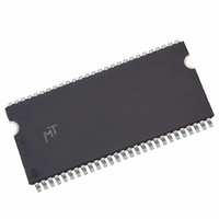
MT48LC32M8A2P-7E:D Micron Technology Inc, MT48LC32M8A2P-7E:D Datasheet - Page 62

MT48LC32M8A2P-7E:D
Manufacturer Part Number
MT48LC32M8A2P-7E:D
Description
IC SDRAM 256MBIT 133MHZ 54TSOP
Manufacturer
Micron Technology Inc
Type
SDRAMr
Datasheet
1.MT48LC16M16A2P-75D_TR.pdf
(92 pages)
Specifications of MT48LC32M8A2P-7E:D
Package / Case
54-TSOP II
Format - Memory
RAM
Memory Type
SDRAM
Memory Size
256M (32M x 8)
Speed
133MHz
Interface
Parallel
Voltage - Supply
3 V ~ 3.6 V
Operating Temperature
0°C ~ 70°C
Access Time
RoHS Compliant
Memory Case Style
TSOP
No. Of Pins
54
Operating Temperature Range
0°C To +70°C
Operating Temperature Max
70°C
Operating Temperature Min
0°C
Organization
32Mx8
Density
256Mb
Address Bus
15b
Access Time (max)
5.4ns
Maximum Clock Rate
143MHz
Operating Supply Voltage (typ)
3.3V
Package Type
TSOP-II
Operating Temp Range
0C to 70C
Operating Supply Voltage (max)
3.6V
Operating Supply Voltage (min)
3V
Supply Current
135mA
Pin Count
54
Mounting
Surface Mount
Operating Temperature Classification
Commercial
Memory Configuration
4 BLK (8M X 8)
Interface Type
LVTTL
Rohs Compliant
Yes
Lead Free Status / RoHS Status
Lead free / RoHS Compliant
Figure 31: WRITE-to-WRITE
PDF: 09005aef8091e6d1
256Mb_sdr.pdf - Rev. N 1/10 EN
Note:
Command
Data for any WRITE burst can be truncated with a subsequent READ command, and
data for a fixed-length WRITE burst can be followed immediately by a READ command.
After the READ command is registered, data input is ignored and WRITEs will not be
executed (see Figure 33 (page 63)). Data n + 1 is either the last of a burst of two or the
last desired data element of a longer burst.
Data for a fixed-length WRITE burst can be followed by or truncated with a PRE-
CHARGE command to the same bank, provided that auto precharge was not activated.
A continuous-page WRITE burst can be truncated with a PRECHARGE command to the
same bank. The PRECHARGE command should be issued
which the last desired input data element is registered. The auto precharge mode re-
quires a
In addition, when truncating a WRITE burst at high clock frequencies (
DQM signal must be used to mask input data for the clock edge prior to and the clock
edge coincident with the PRECHARGE command (see Figure 34 (page 64)). Data n + 1
is either the last of a burst of two or the last desired data element of a longer burst. Fol-
lowing the PRECHARGE command, a subsequent command to the same bank cannot
be issued until
In the case of a fixed-length burst being executed to completion, a PRECHARGE com-
mand issued at the optimum time (as described above) provides the same operation
that would result from the same fixed-length burst with auto precharge. The disadvant-
age of the PRECHARGE command is that it requires that the command and address
buses be available at the appropriate time to issue the command. The advantage of the
PRECHARGE command is that it can be used to truncate fixed-length bursts or continu-
ous page bursts.
Address
1. DQM is LOW. Each WRITE command may be issued to any bank.
CLK
DQ
t
WR of at least one clock with time to complete, regardless of frequency.
WRITE
Bank,
Col n
D
T0
IN
t
RP is met.
NOP
D
T1
IN
62
Don’t Care
WRITE
Bank,
Col b
D
T2
IN
Micron Technology, Inc. reserves the right to change products or specifications without notice.
256Mb: x4, x8, x16 SDRAM
t
WR after the clock edge at
© 1999 Micron Technology, Inc. All rights reserved.
WRITE Operation
t
CK < 15ns), the


