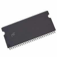
MT48LC32M8A2P-7E:D Micron Technology Inc, MT48LC32M8A2P-7E:D Datasheet - Page 91

MT48LC32M8A2P-7E:D
Manufacturer Part Number
MT48LC32M8A2P-7E:D
Description
IC SDRAM 256MBIT 133MHZ 54TSOP
Manufacturer
Micron Technology Inc
Type
SDRAMr
Datasheet
1.MT48LC16M16A2P-75D_TR.pdf
(92 pages)
Specifications of MT48LC32M8A2P-7E:D
Package / Case
54-TSOP II
Format - Memory
RAM
Memory Type
SDRAM
Memory Size
256M (32M x 8)
Speed
133MHz
Interface
Parallel
Voltage - Supply
3 V ~ 3.6 V
Operating Temperature
0°C ~ 70°C
Access Time
RoHS Compliant
Memory Case Style
TSOP
No. Of Pins
54
Operating Temperature Range
0°C To +70°C
Operating Temperature Max
70°C
Operating Temperature Min
0°C
Organization
32Mx8
Density
256Mb
Address Bus
15b
Access Time (max)
5.4ns
Maximum Clock Rate
143MHz
Operating Supply Voltage (typ)
3.3V
Package Type
TSOP-II
Operating Temp Range
0C to 70C
Operating Supply Voltage (max)
3.6V
Operating Supply Voltage (min)
3V
Supply Current
135mA
Pin Count
54
Mounting
Surface Mount
Operating Temperature Classification
Commercial
Memory Configuration
4 BLK (8M X 8)
Interface Type
LVTTL
Rohs Compliant
Yes
Lead Free Status / RoHS Status
Lead free / RoHS Compliant
Rev. E – 3/02
Rev. D – 7/01
Rev. C – 3/01
PDF: 09005aef8091e6d1
256Mb_sdr.pdf - Rev. N 1/10 EN
• Added 54-ball FBGA package information to front page.
• Added 54-ball FBGA pinout drawing to then-page 3.
• Added 54-ball FBGA package part numbers to then-page 4.
• Added 54-ball FBGA pin descriptions to then-page 10.
• Updated DQM information in 60-ball FGBA pin descriptions on then-page 11.
• Added 54-ball FGBA mech drawing to then-page 59.
• Removed Preliminary status.
• Updated x4 and x8 FBGA row label from Q to R on then-page 2.
• Moved "(to state (A10 LOW})" on then-page 8.
• Updated I
• Added Capacitance table for FBGA to then-page 34.
• Added notes 34-36 for FBGA capacitance (MIN) values different from PC133 on then-
• Changed note 9 and 11 V
• Corrected Initialization waveform (
• Added "FB" FBGA package for x4- and x8-only configurations on then-pages 1 and 3.
• Added new page with FBGA pinout for x4 and x8 configurations on then-page 2.
• Removed -8E speed grade reference on then-pages 1, 11, and 33-55.
• Updated
• Updated Mode Register for A12 from unused to reserved on then-page 10.
• Changed
• Updated MAX -7E/ -75 I
• Added reference "notes appear on page 36" on then-pages 33-35.
• Removed temp reference and added note 5 to all tables.
• Note 21 updated for
• Updated "Don't Care" state of the SELF REFRESH MODE diagram on then-page 41.
• Updated A0-A11 to A0-A9, A11 as A10 is isolated for AP.
• Updated Single READ w/o AP to include note 3 at T3 and T4 NOP cmds on then-page
• Updated Write w/o AP to show
page 36.
1.4V reference level.
44.
page 49.
– I
– I
– I
– I
– I
– I
– I
DD1
DD3
DD4
DD5
DD6
DD7
DD7
t
from 170/160 to 130/120 for -7E/-75.
from 60/60 to 45/40 for -7E/-75.
from 160/160 to 130/130 for -7E/-75.
from 340/320 to 285/270 for -7E/-75.
from 4/4 to 3.5/3.5 for -7E/-75.
from 3/3 to 2.5/2.5 for -7E/-75.
(low power) from 2/2 to 1.5/1.5 for -7E/-75.
t
OH(MIN) value from 2.7ns to 3ns on then-pages 34, 39, 42-48.
DD
RC to
(MAX) Specifications to reflect 71G power edits on then-page 33:
t
RFC for burst AUTO REFRESH commands on then-page 14.
t
CK=ns units vs. MHz reference.
DD5
IH(MIN)
91
from 300/300 to 340/320 respectively on then-page 33.
t
-V
WR = 2 clks and updated note 2 to <Dinm+3> on then-
IL (MAX)
t
CMS and
Micron Technology, Inc. reserves the right to change products or specifications without notice.
test conditions from 0V-3V to 0.8V- 2.0V with
t
CMH reversed) on then-page 37.
256Mb: x4, x8, x16 SDRAM
© 1999 Micron Technology, Inc. All rights reserved.
Revision History


