C8051F005DK Silicon Laboratories Inc, C8051F005DK Datasheet - Page 21
C8051F005DK
Manufacturer Part Number
C8051F005DK
Description
DEV KIT FOR F005/006/007
Manufacturer
Silicon Laboratories Inc
Type
MCUr
Datasheet
1.C8051F005-TB.pdf
(171 pages)
Specifications of C8051F005DK
Contents
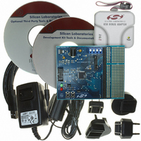
Evaluation Board, Power Supply, USB Cables, Adapter and Documentation
Processor To Be Evaluated
C8051F01x
Interface Type
USB
Silicon Manufacturer
Silicon Labs
Core Architecture
8051
Silicon Core Number
C8051F005
Silicon Family Name
C8051F00x
Lead Free Status / RoHS Status
Contains lead / RoHS non-compliant
For Use With/related Products
Silicon Laboratories C8051 F005/006/007
Lead Free Status / Rohs Status
Lead free / RoHS Compliant
Other names
336-1188
Available stocks
Company
Part Number
Manufacturer
Quantity
Price
Company:

Part Number:
C8051F005DK
Manufacturer:
SiliconL
Quantity:
1


4. PINOUT AND PACKAGE DEFINITIONS
21
VDD
DGND
AV+
AGND
TCK
TMS
TDI
TDO
XTAL1
XTAL2
/RST
VREF
CP0+
CP0-
CP1+
CP1-
DAC0
DAC1
AIN0
AIN1
AIN2
AIN3
AIN4
AIN5
C8051F000/1/2/5/6/7
C8051F010/1/2/5/6/7
Name
F000
F005
F010
F015
31,
40,
30,
41,
16,
62
61
17
15
22
21
28
29
18
19
20
64
63
10
11
12
5,
6
4
3
2
1
7
8
9
Pin Numbers
F001
F006
F011
F016
23,
22,
33,
27,
13,
44,
32
19
43
12
18
17
20
21
14
15
16
45
46
48
47
3
2
1
4
5
6
7
8
9
F002
F007
F012
F017
18,
17,
20
21
29
30
14
13
15
16
10
11
12
32
31
9,
8,
3
2
1
4
5
6
7
D In
D In
D In
D Out
A In
A Out
D I/O
A I/O
A In
A In
A In
A In
A Out
A Out
A In
A In
A In
A In
A In
A In
Type
Table 4.1. Pin Definitions
Description
Digital Voltage Supply.
Digital Ground.
Positive Analog Voltage Supply.
Analog Ground.
JTAG Test Clock with internal pull-up.
JTAG Test-Mode Select with internal pull-up.
JTAG Test Data Input with internal pull-up. TDI is latched on a rising edge of
TCK.
JTAG Test Data Output with internal pull-up. Data is shifted out on TDO on
the falling edge of TCK. TDO output is a tri-state driver.
Crystal Input. This pin is the return for the internal oscillator circuit for a
crystal or ceramic resonator. For a precision internal clock, connect a crystal
or ceramic resonator from XTAL1 to XTAL2. If overdriven by an external
CMOS clock, this becomes the system clock.
Crystal Output. This pin is the excitation driver for a crystal or ceramic
resonator.
Chip Reset. Open-drain output of internal Voltage Supply monitor. Is driven
low when VDD is < 2.7V. An external source can force a system reset by
driving this pin low.
Voltage Reference. When configured as an input, this pin is the voltage
reference for the MCU. Otherwise, the internal reference drives this pin.
Comparator 0 Non-Inverting Input.
Comparator 0 Inverting Input.
Comparator 1 Non-Inverting Input.
Comparator 1 Inverting Input.
Digital to Analog Converter Output 0. The DAC0 voltage output. (See
Section 7 DAC Specification for complete description).
Digital to Analog Converter Output 1. The DAC1 voltage output. (See
Section 7 DAC Specification for complete description).
Analog Mux Channel Input 0. (See ADC Specification for complete
description).
Analog Mux Channel Input 1. (See ADC Specification for complete
description).
Analog Mux Channel Input 2. (See ADC Specification for complete
description).
Analog Mux Channel Input 3. (See ADC Specification for complete
description).
Analog Mux Channel Input 4. (See ADC Specification for complete
description).
Analog Mux Channel Input 5. (See ADC Specification for complete
description).
Rev. 1.7
Related parts for C8051F005DK
Image
Part Number
Description
Manufacturer
Datasheet
Request
R

Part Number:
Description:
SMD/C°/SINGLE-ENDED OUTPUT SILICON OSCILLATOR
Manufacturer:
Silicon Laboratories Inc
Part Number:
Description:
Manufacturer:
Silicon Laboratories Inc
Datasheet:
Part Number:
Description:
N/A N/A/SI4010 AES KEYFOB DEMO WITH LCD RX
Manufacturer:
Silicon Laboratories Inc
Datasheet:
Part Number:
Description:
N/A N/A/SI4010 SIMPLIFIED KEY FOB DEMO WITH LED RX
Manufacturer:
Silicon Laboratories Inc
Datasheet:
Part Number:
Description:
N/A/-40 TO 85 OC/EZLINK MODULE; F930/4432 HIGH BAND (REV E/B1)
Manufacturer:
Silicon Laboratories Inc
Part Number:
Description:
EZLink Module; F930/4432 Low Band (rev e/B1)
Manufacturer:
Silicon Laboratories Inc
Part Number:
Description:
I°/4460 10 DBM RADIO TEST CARD 434 MHZ
Manufacturer:
Silicon Laboratories Inc
Part Number:
Description:
I°/4461 14 DBM RADIO TEST CARD 868 MHZ
Manufacturer:
Silicon Laboratories Inc
Part Number:
Description:
I°/4463 20 DBM RFSWITCH RADIO TEST CARD 460 MHZ
Manufacturer:
Silicon Laboratories Inc
Part Number:
Description:
I°/4463 20 DBM RADIO TEST CARD 868 MHZ
Manufacturer:
Silicon Laboratories Inc
Part Number:
Description:
I°/4463 27 DBM RADIO TEST CARD 868 MHZ
Manufacturer:
Silicon Laboratories Inc
Part Number:
Description:
I°/4463 SKYWORKS 30 DBM RADIO TEST CARD 915 MHZ
Manufacturer:
Silicon Laboratories Inc
Part Number:
Description:
N/A N/A/-40 TO 85 OC/4463 RFMD 30 DBM RADIO TEST CARD 915 MHZ
Manufacturer:
Silicon Laboratories Inc
Part Number:
Description:
I°/4463 20 DBM RADIO TEST CARD 169 MHZ
Manufacturer:
Silicon Laboratories Inc