C8051F005DK Silicon Laboratories Inc, C8051F005DK Datasheet - Page 69
C8051F005DK
Manufacturer Part Number
C8051F005DK
Description
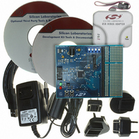
DEV KIT FOR F005/006/007
Manufacturer
Silicon Laboratories Inc
Type
MCUr
Datasheet
1.C8051F005-TB.pdf
(171 pages)
Specifications of C8051F005DK
Contents
Evaluation Board, Power Supply, USB Cables, Adapter and Documentation
Processor To Be Evaluated
C8051F01x
Interface Type
USB
Silicon Manufacturer
Silicon Labs
Core Architecture
8051
Silicon Core Number
C8051F005
Silicon Family Name
C8051F00x
Lead Free Status / RoHS Status
Contains lead / RoHS non-compliant
For Use With/related Products
Silicon Laboratories C8051 F005/006/007
Lead Free Status / Rohs Status
Lead free / RoHS Compliant
Other names
336-1188
Available stocks
Company
Part Number
Manufacturer
Quantity
Price
Company:

Part Number:
C8051F005DK
Manufacturer:
SiliconL
Quantity:
1


10.2.5. Stack
A programmer’s stack can be located anywhere in the 256-byte data memory. The stack area is designated using
the Stack Pointer (SP, 0x81) SFR. The SP will point to the last location used. The next value pushed on the stack is
placed at SP+1 and then SP is incremented. A reset initializes the stack pointer to location 0x07. Therefore, the
first value pushed on the stack is placed at location 0x08, which is also the first register (R0) of register bank 1.
Thus, if more than one register bank is to be used, the SP should be initialized to a location in the data memory not
being used for data storage. The stack depth can extend up to 256 bytes.
The MCUs also have built-in hardware for a stack record. The stack record is a 32-bit shift register, where each
Push or increment SP pushes one record bit onto the register, and each Call or interrupt pushes two record bits onto
the register. (A Pop or decrement SP pops one record bit, and a Return pops two record bits, also.) The stack
record circuitry can also detect an overflow or underflow on the Stack, and can notify the debug software even with
the MCU running full-speed debug.
69
C8051F000/1/2/5/6/7
C8051F010/1/2/5/6/7
0x7DFF
0x7FFF
0x7E00
0x807F
0x8000
0x0000
PROGRAM MEMORY
Programmable in 512
128 Byte ISP FLASH
Byte Sectors)
RESERVED
(In-System
FLASH
Figure 10.2. Memory Map
0xFFFF
0x0FFF
0x17FF
0x07FF
0xF800
0x1000
0x0800
0x0000
0xFF
0x7F
0x2F
0x1F
0x80
0x30
0x20
0x00
(same 2048 byte RAM block )
(same 2048 byte RAM block )
(same 2048 byte RAM block )
Rev. 1.7
RAM - 2048 Bytes
(accessable using MOVX
(Indirect Addressing
(Direct and Indirect
EXTERNAL DATA ADDRESS SPACE
General Purpose
INTERNAL DATA ADDRESS SPACE
Upper 128 RAM
Bit Addressable
Addressing)
Registers
command)
Only)
DATA MEMORY
(Direct Addressing Only)
Special Function
Lower 128 RAM
(Direct and Indirect
Addressing)
Register's
The same 2048 byte RAM
block can be addressed on
2k boundaries throughout
the 64k External Data
Memory space.
Related parts for C8051F005DK
Image
Part Number
Description
Manufacturer
Datasheet
Request
R

Part Number:
Description:
SMD/C°/SINGLE-ENDED OUTPUT SILICON OSCILLATOR
Manufacturer:
Silicon Laboratories Inc
Part Number:
Description:
Manufacturer:
Silicon Laboratories Inc
Datasheet:
Part Number:
Description:
N/A N/A/SI4010 AES KEYFOB DEMO WITH LCD RX
Manufacturer:
Silicon Laboratories Inc
Datasheet:
Part Number:
Description:
N/A N/A/SI4010 SIMPLIFIED KEY FOB DEMO WITH LED RX
Manufacturer:
Silicon Laboratories Inc
Datasheet:
Part Number:
Description:
N/A/-40 TO 85 OC/EZLINK MODULE; F930/4432 HIGH BAND (REV E/B1)
Manufacturer:
Silicon Laboratories Inc
Part Number:
Description:
EZLink Module; F930/4432 Low Band (rev e/B1)
Manufacturer:
Silicon Laboratories Inc
Part Number:
Description:
I°/4460 10 DBM RADIO TEST CARD 434 MHZ
Manufacturer:
Silicon Laboratories Inc
Part Number:
Description:
I°/4461 14 DBM RADIO TEST CARD 868 MHZ
Manufacturer:
Silicon Laboratories Inc
Part Number:
Description:
I°/4463 20 DBM RFSWITCH RADIO TEST CARD 460 MHZ
Manufacturer:
Silicon Laboratories Inc
Part Number:
Description:
I°/4463 20 DBM RADIO TEST CARD 868 MHZ
Manufacturer:
Silicon Laboratories Inc
Part Number:
Description:
I°/4463 27 DBM RADIO TEST CARD 868 MHZ
Manufacturer:
Silicon Laboratories Inc
Part Number:
Description:
I°/4463 SKYWORKS 30 DBM RADIO TEST CARD 915 MHZ
Manufacturer:
Silicon Laboratories Inc
Part Number:
Description:
N/A N/A/-40 TO 85 OC/4463 RFMD 30 DBM RADIO TEST CARD 915 MHZ
Manufacturer:
Silicon Laboratories Inc
Part Number:
Description:
I°/4463 20 DBM RADIO TEST CARD 169 MHZ
Manufacturer:
Silicon Laboratories Inc