C8051F005DK Silicon Laboratories Inc, C8051F005DK Datasheet - Page 88
C8051F005DK
Manufacturer Part Number
C8051F005DK
Description
DEV KIT FOR F005/006/007
Manufacturer
Silicon Laboratories Inc
Type
MCUr
Datasheet
1.C8051F005-TB.pdf
(171 pages)
Specifications of C8051F005DK
Contents
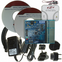
Evaluation Board, Power Supply, USB Cables, Adapter and Documentation
Processor To Be Evaluated
C8051F01x
Interface Type
USB
Silicon Manufacturer
Silicon Labs
Core Architecture
8051
Silicon Core Number
C8051F005
Silicon Family Name
C8051F00x
Lead Free Status / RoHS Status
Contains lead / RoHS non-compliant
For Use With/related Products
Silicon Laboratories C8051 F005/006/007
Lead Free Status / Rohs Status
Lead free / RoHS Compliant
Other names
336-1188
Available stocks
Company
Part Number
Manufacturer
Quantity
Price
Company:

Part Number:
C8051F005DK
Manufacturer:
SiliconL
Quantity:
1


11.2.
The Flash memory can be used for non-volatile data storage as well as program code. This allows data such as
calibration coefficients to be calculated and stored at run time. Data is written using the MOVX instruction and
read using the MOVC instruction.
The MCU incorporates an additional 128-byte sector of Flash memory located at 0x8000 – 0x807F. This sector can
be used for program code or data storage. However, its smaller sector size makes it particularly well suited as
general purpose, non-volatile scratchpad memory. Even though Flash memory can be written a single byte at a
time, an entire sector must be erased first. In order to change a single byte of a multi-byte data set, the data must be
moved to temporary storage. Next, the sector is erased, the data set updated and the data set returned to the original
sector. The 128-byte sector-size facilitates updating data without wasting program memory space by allowing the
use of internal data RAM for temporary storage. (A normal 512-byte sector is too large to be stored in the 256-byte
internal data memory.)
11.3.
The CIP-51 provides security options to protect the Flash memory from inadvertent modification by software as
well as prevent the viewing of proprietary program code and constants.
(PSCTL.0) and the Program Store Erase Enable (PSCTL.1) bits protect the Flash memory from accidental
modification by software. These bits must be explicitly set to logic 1 before software can modify the Flash memory.
Additional security features prevent proprietary program code and data constants from being read or altered across
the JTAG interface or by software running on the system controller.
A set of security lock bytes stored at 0x7DFE and 0x7DFF protect the Flash program memory from being read or
altered across the JTAG interface. Each bit in a security lock-byte protects one 4kbyte block of memory. Clearing
a bit to logic 0 in a Read lock byte prevents the corresponding block of Flash memory from being read across the
JTAG interface. Clearing a bit in the Write/Erase lock byte protects the block from JTAG erasures and/or writes.
The Read lock byte is at location 0x7DFF. The Write/Erase lock byte is located at 0x7DFE. Figure 11.2 shows the
location and bit definitions of the security bytes. The 512-byte sector containing the lock bytes can be written to,
but not erased by software. Writing to the reserved area should not be performed.
Bits7-2: UNUSED. Read = 000000b, Write = don’t care.
Bit1:
Bit0:
R/W
Bit7
-
Non-volatile Data Storage
Security Options
Setting this bit allows an entire page of the Flash program memory to be erased provided
the PSWE bit is also set. After setting this bit, a write to Flash memory using the MOVX
instruction will erase the entire page that contains the location addressed by the MOVX
instruction. The value of the data byte written does not matter.
0: Flash program memory erasure disabled.
1: Flash program memory erasure enabled.
Setting this bit allows writing a byte of data to the Flash program memory using the
MOVX instruction. The location must be erased before writing data.
0: Write to Flash program memory disabled.
1: Write to Flash program memory enabled.
PSEE: Program Store Erase Enable.
PSWE: Program Store Write Enable.
R/W
Bit6
-
Figure 11.1. PSCTL: Program Store RW Control
R/W
Bit5
-
R/W
Bit4
-
Rev. 1.7
R/W
Bit3
-
R/W
Bit2
-
C8051F000/1/2/5/6/7
C8051F010/1/2/5/6/7
The Program Store Write Enable
PSEE
R/W
Bit1
PSWE
R/W
Bit0
SFR Address:
Reset Value
00000000
0x8F
88
Related parts for C8051F005DK
Image
Part Number
Description
Manufacturer
Datasheet
Request
R

Part Number:
Description:
SMD/C°/SINGLE-ENDED OUTPUT SILICON OSCILLATOR
Manufacturer:
Silicon Laboratories Inc
Part Number:
Description:
Manufacturer:
Silicon Laboratories Inc
Datasheet:
Part Number:
Description:
N/A N/A/SI4010 AES KEYFOB DEMO WITH LCD RX
Manufacturer:
Silicon Laboratories Inc
Datasheet:
Part Number:
Description:
N/A N/A/SI4010 SIMPLIFIED KEY FOB DEMO WITH LED RX
Manufacturer:
Silicon Laboratories Inc
Datasheet:
Part Number:
Description:
N/A/-40 TO 85 OC/EZLINK MODULE; F930/4432 HIGH BAND (REV E/B1)
Manufacturer:
Silicon Laboratories Inc
Part Number:
Description:
EZLink Module; F930/4432 Low Band (rev e/B1)
Manufacturer:
Silicon Laboratories Inc
Part Number:
Description:
I°/4460 10 DBM RADIO TEST CARD 434 MHZ
Manufacturer:
Silicon Laboratories Inc
Part Number:
Description:
I°/4461 14 DBM RADIO TEST CARD 868 MHZ
Manufacturer:
Silicon Laboratories Inc
Part Number:
Description:
I°/4463 20 DBM RFSWITCH RADIO TEST CARD 460 MHZ
Manufacturer:
Silicon Laboratories Inc
Part Number:
Description:
I°/4463 20 DBM RADIO TEST CARD 868 MHZ
Manufacturer:
Silicon Laboratories Inc
Part Number:
Description:
I°/4463 27 DBM RADIO TEST CARD 868 MHZ
Manufacturer:
Silicon Laboratories Inc
Part Number:
Description:
I°/4463 SKYWORKS 30 DBM RADIO TEST CARD 915 MHZ
Manufacturer:
Silicon Laboratories Inc
Part Number:
Description:
N/A N/A/-40 TO 85 OC/4463 RFMD 30 DBM RADIO TEST CARD 915 MHZ
Manufacturer:
Silicon Laboratories Inc
Part Number:
Description:
I°/4463 20 DBM RADIO TEST CARD 169 MHZ
Manufacturer:
Silicon Laboratories Inc