C8051F005DK Silicon Laboratories Inc, C8051F005DK Datasheet - Page 29
C8051F005DK
Manufacturer Part Number
C8051F005DK
Description
DEV KIT FOR F005/006/007
Manufacturer
Silicon Laboratories Inc
Type
MCUr
Datasheet
1.C8051F005-TB.pdf
(171 pages)
Specifications of C8051F005DK
Contents
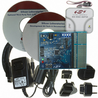
Evaluation Board, Power Supply, USB Cables, Adapter and Documentation
Processor To Be Evaluated
C8051F01x
Interface Type
USB
Silicon Manufacturer
Silicon Labs
Core Architecture
8051
Silicon Core Number
C8051F005
Silicon Family Name
C8051F00x
Lead Free Status / RoHS Status
Contains lead / RoHS non-compliant
For Use With/related Products
Silicon Laboratories C8051 F005/006/007
Lead Free Status / Rohs Status
Lead free / RoHS Compliant
Other names
336-1188
Available stocks
Company
Part Number
Manufacturer
Quantity
Price
Company:

Part Number:
C8051F005DK
Manufacturer:
SiliconL
Quantity:
1


5. ADC (12-Bit, C8051F000/1/2/5/6/7 Only)
The ADC subsystem for the C8051F000/1/2/5/6/7 consists of a 9-channel, configurable analog multiplexer
(AMUX), a programmable gain amplifier (PGA), and a 100ksps, 12-bit successive-approximation-register ADC
with integrated track-and-hold and programmable window detector (see block diagram in Figure 5.1). The AMUX,
PGA, Data Conversion Modes, and Window Detector are all configurable under software control via the Special
Function Register’s shown in Figure 5.1. The ADC subsystem (ADC, track-and-hold and PGA) is enabled only
when the ADCEN bit in the ADC Control register (ADC0CN, Figure 5.7) is set to 1. The ADC subsystem is in low
power shutdown when this bit is 0. The Bias Enable bit (BIASE) in the REF0CN register (see Figure 9.2) must be
set to 1 in order to supply bias to the ADC.
5.1.
Eight of the AMUX channels are available for external measurements while the ninth channel is internally
connected to an on-board temperature sensor (temperature transfer function is shown in Figure 5.3). Note that the
PGA gain is applied to the temperature sensor reading. AMUX input pairs can be programmed to operate in either
the differential or single-ended mode. This allows the user to select the best measurement technique for each input
channel, and even accommodates mode changes “on-the-fly”. The AMUX defaults to all single-ended inputs upon
reset. There are two registers associated with the AMUX: the Channel Selection register AMX0SL (Figure 5.5),
and the Configuration register AMX0CF (Figure 5.4). The table in Figure 5.5 shows AMUX functionality by
channel for each possible configuration. The PGA amplifies the AMUX output signal by an amount determined by
the AMPGN2-0 bits in the ADC Configuration register, ADC0CF (Figure 5.6). The PGA can be software-
programmed for gains of 0.5, 1, 2, 4, 8 or 16. It defaults to unity gain on reset.
29
C8051F000/1/2/5/6/7
C8051F010/1/2/5/6/7
AIN0
AIN1
AIN2
AIN3
AIN4
AIN5
AIN6
AIN7
Analog Multiplexer and PGA
SENSOR
AGND
TEMP
AMX0CF
ADC0GTH
Figure 5.1. 12-Bit ADC Functional Block Diagram
+
+
+
+
-
-
-
-
AMUX
(SE or
9-to-1
DIFF)
AMX0SL
ADC0GTL
X
+
-
AV+
ADCEN
Rev. 1.7
AGND
ADC0CF
ADC0LTH
ADC
12-Bit
AV+
SAR
ADC0CN
ADC0LTL
12
24
12
COMB
LOGIC
ADWINT
Related parts for C8051F005DK
Image
Part Number
Description
Manufacturer
Datasheet
Request
R

Part Number:
Description:
SMD/C°/SINGLE-ENDED OUTPUT SILICON OSCILLATOR
Manufacturer:
Silicon Laboratories Inc
Part Number:
Description:
Manufacturer:
Silicon Laboratories Inc
Datasheet:
Part Number:
Description:
N/A N/A/SI4010 AES KEYFOB DEMO WITH LCD RX
Manufacturer:
Silicon Laboratories Inc
Datasheet:
Part Number:
Description:
N/A N/A/SI4010 SIMPLIFIED KEY FOB DEMO WITH LED RX
Manufacturer:
Silicon Laboratories Inc
Datasheet:
Part Number:
Description:
N/A/-40 TO 85 OC/EZLINK MODULE; F930/4432 HIGH BAND (REV E/B1)
Manufacturer:
Silicon Laboratories Inc
Part Number:
Description:
EZLink Module; F930/4432 Low Band (rev e/B1)
Manufacturer:
Silicon Laboratories Inc
Part Number:
Description:
I°/4460 10 DBM RADIO TEST CARD 434 MHZ
Manufacturer:
Silicon Laboratories Inc
Part Number:
Description:
I°/4461 14 DBM RADIO TEST CARD 868 MHZ
Manufacturer:
Silicon Laboratories Inc
Part Number:
Description:
I°/4463 20 DBM RFSWITCH RADIO TEST CARD 460 MHZ
Manufacturer:
Silicon Laboratories Inc
Part Number:
Description:
I°/4463 20 DBM RADIO TEST CARD 868 MHZ
Manufacturer:
Silicon Laboratories Inc
Part Number:
Description:
I°/4463 27 DBM RADIO TEST CARD 868 MHZ
Manufacturer:
Silicon Laboratories Inc
Part Number:
Description:
I°/4463 SKYWORKS 30 DBM RADIO TEST CARD 915 MHZ
Manufacturer:
Silicon Laboratories Inc
Part Number:
Description:
N/A N/A/-40 TO 85 OC/4463 RFMD 30 DBM RADIO TEST CARD 915 MHZ
Manufacturer:
Silicon Laboratories Inc
Part Number:
Description:
I°/4463 20 DBM RADIO TEST CARD 169 MHZ
Manufacturer:
Silicon Laboratories Inc