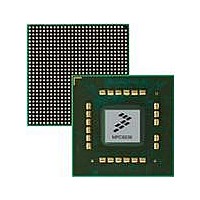
MPC8536DS Freescale Semiconductor, MPC8536DS Datasheet - Page 719

MPC8536DS
Manufacturer Part Number
MPC8536DS
Description
BOARD DEV SYSTEM MPC8536E
Manufacturer
Freescale Semiconductor
Series
PowerQUICC III™r
Type
MPUr
Datasheets
1.MPC8536EBVTAVLA.pdf
(127 pages)
2.MPC8536EBVTAVLA.pdf
(1706 pages)
3.MPC8536DS.pdf
(2 pages)
4.MPC8536DS.pdf
(126 pages)
Specifications of MPC8536DS
Contents
Board, Software and Documentation
Processor Series
MPC85xx
Core
e500
Data Bus Width
32 bit
Maximum Clock Frequency
667 MHz
Operating Supply Voltage
- 0.3 V to + 1.21 V
Maximum Operating Temperature
+ 105 C
Data Ram Size
32 KB
Interface Type
SPI, USB
Program Memory Type
DDR2, DDR3, SDRAM
Core Size
32 Bit
Program Memory Size
544KB
Cpu Speed
1.5GHz
Digital Ic Case Style
BGA
No. Of Pins
783
Supply Voltage Range
0.95V To 1.05V
Rohs Compliant
Yes
For Use With/related Products
MPC8536
Lead Free Status / RoHS Status
Lead free / RoHS Compliant
- MPC8536EBVTAVLA PDF datasheet
- MPC8536EBVTAVLA PDF datasheet #2
- MPC8536DS PDF datasheet #3
- MPC8536DS PDF datasheet #4
- Current page: 719 of 1706
- Download datasheet (15Mb)
Any transfers that do not naturally fit single or burst transfers are synthesized as a series of single transfers.
These accesses are treated by the UPM as back-to-back, single-beat transfers. Burst transfers can also be
inhibited by setting ORn[BI]. Burst performance can be achieved by ensuring that UPM transactions are
32-byte aligned with a transaction size being some multiple of 32-bytes, which is a natural fit for
cache-line transfers, for example.
13.4.4.1.2
Each UPM contains a refresh timer that can be programmed to generate refresh service requests of a
particular pattern in the RAM array.
memory refresh timer request generation. The UPM refresh timer register (LURT) defines the period for
the timers associated with all three UPMs.
By default, all local bus refreshes are performed using the refresh pattern of UPMA. This means that if
refresh is required, MAMR[RFEN] must be set. It also means that only one refresh routine should be
programmed and be placed in UPMA, which serves as the refresh executor. Any banks assigned to a UPM
are provided with the common UPMA refresh pattern if the RFEN bit of the corresponding UPM is set,
concurrently. UPMA assigned banks, therefore, always receive refresh services when MAMR[RFEN] is
set, while UPMB and UPMC assigned banks also receive (the same) refresh services if the corresponding
MxMR[RFEN] bits are set. In this scenario, more than one chip select may assert at the same time, as
refresh pattern runs for all banks assigned to UPM with RFEN bit set.
13.4.4.1.3
Software can start a request to the UPM by issuing a RUN command to the UPM. Some memory devices
have their own signal handshaking protocol to put them into special modes, such as self-refresh mode.
For these special cycles, the user creates a special RAM pattern that can be stored in any unused areas in
the UPM RAM. Then a RUN command is used to run the cycle. The UPM runs the pattern beginning at
the specified RAM location until it encounters a RAM word with its LAST bit set. The RUN command is
issued by setting MxMR[OP] = 11 and accessing UPMn memory region with any write transaction that
hits the corresponding UPM machine. MxMR[MAD] determines the starting address in the RAM array for
the pattern.
Note that transfer acknowledges (UTA bit in the RAM word) are ignored for software (RUN command)
requests, and hence the LAD signals remain high-impedance unless the normal initial LALE occurs or the
RUN pattern causes assertion of LALE to occur on changes to the RAM word AMX field.
13.4.4.1.4
When the eLBC under UPM control initiates an access to a memory device and an exception occurs (bus
monitor time-out), the UPM provides a mechanism by which memory control signals can meet the device’s
Freescale Semiconductor
System
Clock
UPM Refresh Timer Requests
Software Requests—RUN Command
Exception Requests
MPC8536E PowerQUICC III Integrated Processor Reference Manual, Rev. 1
Figure 13-63. Memory Refresh Timer Request Block Diagram
PTP Prescaling
Figure 13-63
shows the clock division hardware associated with
Divide by LURT
UPM refresh timer request
Enhanced Local Bus Controller
13-77
Related parts for MPC8536DS
Image
Part Number
Description
Manufacturer
Datasheet
Request
R
Part Number:
Description:
Manufacturer:
Freescale Semiconductor, Inc
Datasheet:
Part Number:
Description:
Manufacturer:
Freescale Semiconductor, Inc
Datasheet:
Part Number:
Description:
Manufacturer:
Freescale Semiconductor, Inc
Datasheet:
Part Number:
Description:
Manufacturer:
Freescale Semiconductor, Inc
Datasheet:
Part Number:
Description:
Manufacturer:
Freescale Semiconductor, Inc
Datasheet:
Part Number:
Description:
Manufacturer:
Freescale Semiconductor, Inc
Datasheet:
Part Number:
Description:
Manufacturer:
Freescale Semiconductor, Inc
Datasheet:
Part Number:
Description:
Manufacturer:
Freescale Semiconductor, Inc
Datasheet:
Part Number:
Description:
Manufacturer:
Freescale Semiconductor, Inc
Datasheet:
Part Number:
Description:
Manufacturer:
Freescale Semiconductor, Inc
Datasheet:
Part Number:
Description:
Manufacturer:
Freescale Semiconductor, Inc
Datasheet:
Part Number:
Description:
Manufacturer:
Freescale Semiconductor, Inc
Datasheet:
Part Number:
Description:
Manufacturer:
Freescale Semiconductor, Inc
Datasheet:
Part Number:
Description:
Manufacturer:
Freescale Semiconductor, Inc
Datasheet:
Part Number:
Description:
Manufacturer:
Freescale Semiconductor, Inc
Datasheet:


