AN2131-DK001 Cypress Semiconductor Corp, AN2131-DK001 Datasheet - Page 158
AN2131-DK001
Manufacturer Part Number
AN2131-DK001
Description
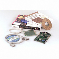
KIT EZ-USB DEVELOPMENT BOARD
Manufacturer
Cypress Semiconductor Corp
Datasheet
1.AN2131SC.pdf
(334 pages)
Specifications of AN2131-DK001
Lead Free Status / RoHS Status
Contains lead / RoHS non-compliant
Other names
428-1333


The timing choices for fast write pulses (FWR#) are shown in Figure 8-11. The 8051 can
extend the output data and widths of these pulses by setting cycle stretch values greater
than zero in the 8051 Clock Control Register CKCON (at SFR location 0x8E). The top
five waveforms show the fastest write timings, with a stretch value of 000, which per-
forms the write in eight 8051 clocks. The bottom five waveforms show the same wave-
forms with a stretch value of 001.
8.7.2 Fast Read Waveforms
The timing choices for fast read pulses (FRD#) are shown in Figure 8-12. Read Strobe
waveforms for stretch values of 000 and 001 are indicated. Although two of the read
strobe widths can be extended using stretch values greater than 000, the times that the
input data is sampled by the EZ-USB core remains the same as shown.
EZ-USB TRM v1.9
FRD#[00]
FRD#[01]
FRD#[10]
FRD#[10]
FRD#[11]
FRD#[11]
OSC24
D[7..0]
D[7..0]
D[7..0]
D[7..0]
41.66 ns
tCL
Note: If WPOL=1 the waveforms are inverted
Figure 8-12. Fast Read Timing
[nn] = RMOD1:RMOD0, RPOL=0
In
Chapter 8. EZ-USB CPU
In
In
In
stretch=000, 001
stretch=000, 001
stretch=000
stretch=001
stretch=000
stretch=001
Page 8-13
Related parts for AN2131-DK001
Image
Part Number
Description
Manufacturer
Datasheet
Request
R

Part Number:
Description:
Two Chip Voltage Controlled Amplifier & Video Switch
Manufacturer:
Analog Devices

Part Number:
Description:
Manufacturer:
Cypress Semiconductor Corp
Datasheet:
Part Number:
Description:
Manufacturer:
Cypress Semiconductor Corp
Datasheet:
Part Number:
Description:
Manufacturer:
Cypress Semiconductor Corp
Datasheet:
Part Number:
Description:
Manufacturer:
Cypress Semiconductor Corp
Datasheet:
Part Number:
Description:
Manufacturer:
Cypress Semiconductor Corp
Datasheet: