AN2131-DK001 Cypress Semiconductor Corp, AN2131-DK001 Datasheet - Page 299
AN2131-DK001
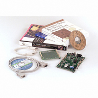
Manufacturer Part Number
AN2131-DK001
Description
KIT EZ-USB DEVELOPMENT BOARD
Manufacturer
Cypress Semiconductor Corp
Datasheet
1.AN2131SC.pdf
(334 pages)
Specifications of AN2131-DK001
Lead Free Status / RoHS Status
Contains lead / RoHS non-compliant
Other names
428-1333


The upper 3 bits of TL0 (or TL1) are indeterminate in mode 0 and must be masked when the
software evaluates the register.
T0M (or T1M)
Divide by 12
0
CLK24
0
CLK
TL0 (or TL1)
1
7
4
0
C/ T
Divide by 4
1
Mode 0
T0 (or T1) pin
Mode 1
TR0 (or TR1)
TH0 (or TH1)
7
0
GATE
INT0# pin
TF0 (or TF1)
INT
(or INT1#)
To Serial Port
(Timer 1 only)
Figure C-1. Timer 0/1 - Modes 0 and 1
C.2.4 Mode 1
Mode 1 operation is the same for Timer 0 and Timer 1. In mode 1, the timer is configured as a
16-bit counter. As illustrated in Figure C-1., all 8 bits of the LSB register (TL0 or TL1) are
used. The counter rolls over to all zeros when the count increments from FFFFh. Otherwise,
mode 1 operation is the same as mode 0.
EZ-USB TRM v1.9
Appendix C: 8051 Hardware Description
C - 3
Related parts for AN2131-DK001
Image
Part Number
Description
Manufacturer
Datasheet
Request
R

Part Number:
Description:
Two Chip Voltage Controlled Amplifier & Video Switch
Manufacturer:
Analog Devices

Part Number:
Description:
Manufacturer:
Cypress Semiconductor Corp
Datasheet:
Part Number:
Description:
Manufacturer:
Cypress Semiconductor Corp
Datasheet:
Part Number:
Description:
Manufacturer:
Cypress Semiconductor Corp
Datasheet:
Part Number:
Description:
Manufacturer:
Cypress Semiconductor Corp
Datasheet:
Part Number:
Description:
Manufacturer:
Cypress Semiconductor Corp
Datasheet: