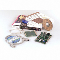
AN2131-DK001 Cypress Semiconductor Corp, AN2131-DK001 Datasheet - Page 283

AN2131-DK001
Manufacturer Part Number
AN2131-DK001
Description
KIT EZ-USB DEVELOPMENT BOARD
Manufacturer
Cypress Semiconductor Corp
Datasheet
1.AN2131SC.pdf
(334 pages)
Specifications of AN2131-DK001
Lead Free Status / RoHS Status
Contains lead / RoHS non-compliant
Other names
428-1333
- Current page: 283 of 334
- Download datasheet (2Mb)
B.1.2 Instruction Set
All 8051 instructions are binary code compatible and perform the same functions as they do
with the industry standard 8051. The effects of these instructions on bits, flags, and other
status functions is identical to the industry standard 8051. However, the timing of the
instructions is different, both in terms of number of clock cycles per instruction cycle and
timing within the instruction cycle.
Figure B-2 lists the 8051 instruction set and the number of instruction cycles required to
complete each instruction. Table B-1. defines the symbols and mnemonics used in Table B-2.
EZ-USB v1.9
Bank
Select
(PSW bits
4,3)
11
10
01
00
7Fh
30h
2Fh
20h
1Fh
18h
17h
10h
0Fh
08h
07h
00h
7F
07
Lower 128 bytes
Bit-Addressable
Registers
.
.
.
Direct RAM
Bank 0
Bank 3
Bank 2
Bank 1
. . .
. . .
Appendix B: 8051 Architectural Overview
78
00
Figure B-2 Internal RAM Organization
00h
FFh
80h
7Fh
Upper 128
bytes
(optional)
Lower 128
bytes
Direct or indirect addressing
Indirect addressing only
Direct addressing only
SFR space
FFh
80h
B - 3
Related parts for AN2131-DK001
Image
Part Number
Description
Manufacturer
Datasheet
Request
R

Part Number:
Description:
Two Chip Voltage Controlled Amplifier & Video Switch
Manufacturer:
Analog Devices
Part Number:
Description:
Manufacturer:
Cypress Semiconductor Corp
Datasheet:
Part Number:
Description:
Manufacturer:
Cypress Semiconductor Corp
Datasheet:
Part Number:
Description:
Manufacturer:
Cypress Semiconductor Corp
Datasheet:
Part Number:
Description:
Manufacturer:
Cypress Semiconductor Corp
Datasheet:
Part Number:
Description:
Manufacturer:
Cypress Semiconductor Corp
Datasheet:


