AN2131-DK001 Cypress Semiconductor Corp, AN2131-DK001 Datasheet - Page 55
AN2131-DK001
Manufacturer Part Number
AN2131-DK001
Description
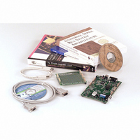
KIT EZ-USB DEVELOPMENT BOARD
Manufacturer
Cypress Semiconductor Corp
Datasheet
1.AN2131SC.pdf
(334 pages)
Specifications of AN2131-DK001
Lead Free Status / RoHS Status
Contains lead / RoHS non-compliant
Other names
428-1333


Figure 3-1 illustrates the two internal EZ-USB RAM regions. 6,976 bytes of general-pur-
pose RAM occupy addresses 0x0000-0x1B3F. This RAM is loadable by the EZ-USB
core or I
The EZ-USB EA (External Access) pin controls where the bottom segment of code
(PSEN) memory is located—inside (EA=0) or outside (EA=1) the EZ-USB chip. If the
EZ pin is tied low, the EZ-USB core internally ORs the two 8051 read signals PSEN and
RD for this region, so that code and data share the 0x0000-0x1B3F memory space. IF
EA=1, all code (PSEN) memory is external.
1,024 bytes of RAM at 0x7B40-0x7F3F implement the sixteen bulk endpoint buffers. 192
additional bytes at 0x7F40-0x7FFF contain the USB control registers. The 8051 reads and
writes this memory using the MOVX instruction. In the 8-KB RAM EZ-USB version, the
1,024 bulk endpoint buffer bytes at 0x7B40-0x7F3F also appear at 0x1B40-0x1F3F. This
aliasing allows unused bulk endpoint buffer memory to be added contiguously to the data
memory, as illustrated Figure 3-3. The memory space at 0x1F40-0x1FFF should not be
used.
Even though the 8051 can access EZ-USB endpoint buffers at either 0x1B40 or 0x7B40,
the firmware should be written to access this memory only at 0x7B40-0x7FFF to maintain
compatibility with future versions of EZ-USB that contain more than 8 KB of RAM.
Future versions will have the bulk buffer space at 0x7B40-0x7F3F only.
Page 3-2
3.2
About 8051 Memory Spaces
The 8051 partitions its memory spaces into code memory and data memory. The 8051
reads code memory using the signal PSEN# (Program Store Enable), reads data memory
using the signal RD# (Data Read) and writes data memory using the signal WR# (Data
Write). The 8051 MOVX (move external) instruction generates RD# or WR# strobes.
PSEN# is a dedicated pin, while the RD# and WR# signals share pins with two IO port
signals: PC7/RD and PC6/WR. Therefore, if expanded memory is used, the port pins
PC7 and PC6 are not available to the system.
8051 Memory
2
C bus EEPROM, and contains 8051 code and data.
Chapter 3. EZ-USB Memory
EZ-USB TRM v1.9
Related parts for AN2131-DK001
Image
Part Number
Description
Manufacturer
Datasheet
Request
R

Part Number:
Description:
Two Chip Voltage Controlled Amplifier & Video Switch
Manufacturer:
Analog Devices

Part Number:
Description:
Manufacturer:
Cypress Semiconductor Corp
Datasheet:
Part Number:
Description:
Manufacturer:
Cypress Semiconductor Corp
Datasheet:
Part Number:
Description:
Manufacturer:
Cypress Semiconductor Corp
Datasheet:
Part Number:
Description:
Manufacturer:
Cypress Semiconductor Corp
Datasheet:
Part Number:
Description:
Manufacturer:
Cypress Semiconductor Corp
Datasheet: