AN2131-DK001 Cypress Semiconductor Corp, AN2131-DK001 Datasheet - Page 290
AN2131-DK001
Manufacturer Part Number
AN2131-DK001
Description
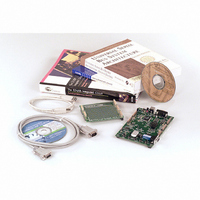
KIT EZ-USB DEVELOPMENT BOARD
Manufacturer
Cypress Semiconductor Corp
Datasheet
1.AN2131SC.pdf
(334 pages)
Specifications of AN2131-DK001
Lead Free Status / RoHS Status
Contains lead / RoHS non-compliant
Other names
428-1333


accesses (bytes) needed to execute the instruction. In most cases, the number of bytes is equal to
the number of instruction cycles required to complete the instruction. However, as indicated,
there are some instructions (for example, DIV and MUL) that require a greater number of
instruction cycles than memory accesses.
By default, the 8051 core timer/counters run at 12 clock cycles per increment so that timer-
based events have the same timing as with the standard 8051. The timers can also be configured
to run at 4 clock cycles per increment to take advantage of the higher speed of the 8051 core.
B.1.4 CPU Timing
As previously stated, an 8051 core instruction cycle consists of 4 CLK24 cycles. Each CLK24
cycle forms a CPU cycle. Therefore, an instruction cycle consists of 4 CPU cycles: C1, C2, C3,
and C4, as illustrated in Figure B-3. Various events occur in each CPU cycle, depending on the
type of instruction being executed. The labels C1, C2, C3, and C4 in timing descriptions refer to
the 4 CPU cycles within a particular instruction cycle.
The execution for instruction n is performed during the fetch of instruction n+1. Data writes
occur during fetch of instruction n+2. The level sensitive interrupts are sampled with the rising
edge of CLK24 at the end of C3.
CLK24
Instruction cycle
n + 1
n + 2
CPU cycle
C2
C1
C3
C1
C4
C2
C3
C4
C1
Figure B-3 CPU Timing for Single-Cycle Instruction
B.1.5 Stretch Memory Cycles (Wait States)
The stretch memory cycle feature enables application software to adjust the speed of data
memory access. The 8051 core can execute the MOVX instruction in as few as 2 instruction
cycles. However, it is sometimes desirable to stretch this value; for example to access slow
memory or slow memory-mapped peripherals such as UARTs or LCDs.
The three LSBs of the Clock Control Register (at SFR location 8Eh) control the stretch value.
You can use stretch values between zero and seven. A stretch value of zero adds zero instruction
cycles, resulting in MOVX instructions executing in two instruction cycles. A stretch value of
seven adds seven instruction cycles, resulting in MOVX instructions executing in nine instruction
cycles. The stretch value can be changed dynamically under program control.
B - 10
Appendix B: 8051 Architectural Overview
EZ-USB TRM v1.9
Related parts for AN2131-DK001
Image
Part Number
Description
Manufacturer
Datasheet
Request
R

Part Number:
Description:
Two Chip Voltage Controlled Amplifier & Video Switch
Manufacturer:
Analog Devices

Part Number:
Description:
Manufacturer:
Cypress Semiconductor Corp
Datasheet:
Part Number:
Description:
Manufacturer:
Cypress Semiconductor Corp
Datasheet:
Part Number:
Description:
Manufacturer:
Cypress Semiconductor Corp
Datasheet:
Part Number:
Description:
Manufacturer:
Cypress Semiconductor Corp
Datasheet:
Part Number:
Description:
Manufacturer:
Cypress Semiconductor Corp
Datasheet: