AN2131-DK001 Cypress Semiconductor Corp, AN2131-DK001 Datasheet - Page 72
AN2131-DK001
Manufacturer Part Number
AN2131-DK001
Description
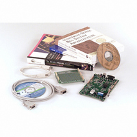
KIT EZ-USB DEVELOPMENT BOARD
Manufacturer
Cypress Semiconductor Corp
Datasheet
1.AN2131SC.pdf
(334 pages)
Specifications of AN2131-DK001
Lead Free Status / RoHS Status
Contains lead / RoHS non-compliant
Other names
428-1333


To read a multiple-byte data record, follow these steps:
* If the I
EZ-USB TRM v1.9
4.9
rupt-driven, and handled by an interrupt service routing. See Section 9.12, "I
rupt” for more details regarding the I
1. Set the START bit.
2. Write the peripheral address and direction=1 (for read) to I2DAT.
3. Wait for DONE=1*. If BERR=1 or ACK=0, terminate by setting STOP=1.
4. Read I2DAT and discard the data. This initiates the first burst of nine SCL pulses
5. Wait for DONE=1*. If BERR=1, terminate by setting STOP=1.
6. Read the data from I2DAT. This initiates another read transfer.
7. Repeat steps 5 and 6 for each byte until ready to read the second-to-last byte.
8. Before reading the second-to-last I2DAT byte, set LASTRD=1.
9. Read the data from I2DAT. With LASTRD=1, this initiates the final byte read on
10. Wait for DONE=1*. If BERR=1, terminate by setting STOP=1.
11. Set STOP=1.
12. Read the last byte from I2DAT immediately (the next instruction) after setting the
to clock in the first byte from the slave.
the I
STOP bit. This retrieves the last data byte without initiating an extra read transac-
tion (nine more SCL pulses) on the I
Receiving I
2
C interrupt (8051 INT3) is enabled, each “Wait for DONE=1” step can be inter-
2
C bus.
2
C Data
Chapter 4. EZ-USB CPU
2
C interrupt.
2
C bus.
2
C Inter-
Page 4-11
Related parts for AN2131-DK001
Image
Part Number
Description
Manufacturer
Datasheet
Request
R

Part Number:
Description:
Two Chip Voltage Controlled Amplifier & Video Switch
Manufacturer:
Analog Devices

Part Number:
Description:
Manufacturer:
Cypress Semiconductor Corp
Datasheet:
Part Number:
Description:
Manufacturer:
Cypress Semiconductor Corp
Datasheet:
Part Number:
Description:
Manufacturer:
Cypress Semiconductor Corp
Datasheet:
Part Number:
Description:
Manufacturer:
Cypress Semiconductor Corp
Datasheet:
Part Number:
Description:
Manufacturer:
Cypress Semiconductor Corp
Datasheet: