AN2131-DK001 Cypress Semiconductor Corp, AN2131-DK001 Datasheet - Page 63
AN2131-DK001
Manufacturer Part Number
AN2131-DK001
Description
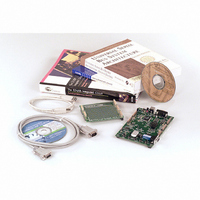
KIT EZ-USB DEVELOPMENT BOARD
Manufacturer
Cypress Semiconductor Corp
Datasheet
1.AN2131SC.pdf
(334 pages)
Specifications of AN2131-DK001
Lead Free Status / RoHS Status
Contains lead / RoHS non-compliant
Other names
428-1333


4.2
IO Ports
OE
OUT
Pin
reg
PINS
Figure 4-1. EZ-USB Input/Output Pin
The EZ-USB family implements its IO ports using memory-mapped registers. This is in
contrast to a standard, which uses SFR bits for input/output.
Figure 4-1 shows the basic structure of an EZ-USB IO pin. Twenty-four IO pins are
grouped into three 8-bit ports named PORTA, PORTB, and PORTC. The AN2131Q has
all three ports, while the AN2131S has PORTB, PORTC, and two PORTA bits. The 8051
accesses IO pins using the three control bits shown in Figure 4-1: OE, OUT, and PINS.
The OUT bit writes output data to a register, the OE bit turns on the output buffer, and the
PINS bit indicates the state of the pin.
To configure a pin as an input, the 8051 sets OE=0 to turn off the output buffer. To config-
ure a pin as an output, the 8051 sets OE=1 to turn on the output buffer, and writes data to
the OUT register. The PINS bit reflects the actual pin value regardless of the value of OE.
A fourth control bit (in PORTACFG, PORTBCFG, PORTCCFG registers) determines
whether a port pin is general-purpose Input/Output (GPIO) as shown in Figure 4-1, or
connected to an alternate 8051 or EZ-USB function. Table 4-1 lists the alternate functions
available on the IO pins. Figure 4-1 shows the registers and bits associated with the IO
ports.
Page 4-2
Chapter 4. EZ-USB CPU
EZ-USB TRM v1.9
Related parts for AN2131-DK001
Image
Part Number
Description
Manufacturer
Datasheet
Request
R

Part Number:
Description:
Two Chip Voltage Controlled Amplifier & Video Switch
Manufacturer:
Analog Devices

Part Number:
Description:
Manufacturer:
Cypress Semiconductor Corp
Datasheet:
Part Number:
Description:
Manufacturer:
Cypress Semiconductor Corp
Datasheet:
Part Number:
Description:
Manufacturer:
Cypress Semiconductor Corp
Datasheet:
Part Number:
Description:
Manufacturer:
Cypress Semiconductor Corp
Datasheet:
Part Number:
Description:
Manufacturer:
Cypress Semiconductor Corp
Datasheet: