AN2131-DK001 Cypress Semiconductor Corp, AN2131-DK001 Datasheet - Page 42
AN2131-DK001
Manufacturer Part Number
AN2131-DK001
Description
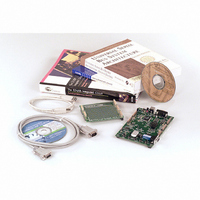
KIT EZ-USB DEVELOPMENT BOARD
Manufacturer
Cypress Semiconductor Corp
Datasheet
1.AN2131SC.pdf
(334 pages)
Specifications of AN2131-DK001
Lead Free Status / RoHS Status
Contains lead / RoHS non-compliant
Other names
428-1333


EZ-USB TRM v1.9
2131Q
71
73
74
75
76
2121S
2122S
2131S
N/A
N/A
N/A
39
40
2125S
2126S
2135S
2136S
N/A
N/A
N/A
39
40
2122T 2126T
N/A
N/A
N/A
44
8
Table 1-3. EZ-USB Series 2100 Pinouts by Pin Function
N/A
N/A
N/A
44
8
PA4 or FWR#
PA5 or FRD#
PA3 or CS#
RXD0OUT
RXD1OUT
PA7 OR
PA6 or
Name
Chapter 1. Introducing EZ-USB
Type
I/O
I/O
I/O
I/O
I/O
Default
(PA3)
(PA4)
(PA5)
(PA6)
(PA7)
I
I
I
I
I
Multiplexed pin whose function is selected by the CS
bit of the PORTACFG register. If CS=0, the pin is
the bi-directional I/O port pin PA3. If CS=1, the pin is
an active-low chip select for external memory. If the
CS# pin is used, it should be externally pulled up to
Vcc to ensure that the write strobe is inactive (high)
at power-on.
Multiplexed pin whose function is selected by the
FWR (Fast Write) bit of the PORTAFCG register. If
FWR=0, the pin is the bi-directional I/O port pin PA4.
If FWR=1, the pin is the write strobe for an external
FIFO. If the FWR# pin is used, it should be exter-
nally pulled up to Vcc to ensure that the write strobe
is inactive (high) at power-on.
Multiplexed pin whose function is selected by the
FRD (Fast Read) bit of the PORTAFCG register. If
FRD=0, the pin is the bi-directional I/O port pin PA5.
If FRD=1, the pin is the read strobe for an external
FIFO. If the FRD# pin is used, it should be exter-
nally pulled up to Vcc to ensure that the write strobe
is inactive (high) at power-on.
Multiplexed pin whose function is selected by the
RXD0OUT bit of the PORTAFCG register. If
RXD0OUT=0 (default), the pin is the bi-directional
I/O port bit PA6. If RXD0OUT=1, the pin is the
active-high RXD0OUT signal from 8051 UART0.
If RXD0OUT is selected and UART0 is in mode 0,
this pin provides the output data for UART0 only
when it is in sync mode. Otherwise, it is a 1.
Multiplexed pin whose function is selected by the
RXD1OUT bit of the PORTAFCG register. If
RXD1OUT=0 (default), the pin is the bi-directional
I/O port bit PA7. If RXD1OUT=1, the pin is the
active-high RXD1OUT signal from 8051 UART1.
When RXD1OUT is selected and UART1 is in mode
0, this pin provides the output data for UaRT1 only
when it is in sync mode. In modes 1, 2, and 3, this
pin is a 1.
Description
Page 1-25
Related parts for AN2131-DK001
Image
Part Number
Description
Manufacturer
Datasheet
Request
R

Part Number:
Description:
Two Chip Voltage Controlled Amplifier & Video Switch
Manufacturer:
Analog Devices

Part Number:
Description:
Manufacturer:
Cypress Semiconductor Corp
Datasheet:
Part Number:
Description:
Manufacturer:
Cypress Semiconductor Corp
Datasheet:
Part Number:
Description:
Manufacturer:
Cypress Semiconductor Corp
Datasheet:
Part Number:
Description:
Manufacturer:
Cypress Semiconductor Corp
Datasheet:
Part Number:
Description:
Manufacturer:
Cypress Semiconductor Corp
Datasheet: