AN2131-DK001 Cypress Semiconductor Corp, AN2131-DK001 Datasheet - Page 68
AN2131-DK001
Manufacturer Part Number
AN2131-DK001
Description
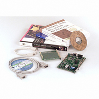
KIT EZ-USB DEVELOPMENT BOARD
Manufacturer
Cypress Semiconductor Corp
Datasheet
1.AN2131SC.pdf
(334 pages)
Specifications of AN2131-DK001
Lead Free Status / RoHS Status
Contains lead / RoHS non-compliant
Other names
428-1333


The first byte of an I
Figure 4-7 shows the format for this first byte, which is sometimes called a control byte.
A master sends the bit sequence shown in Figure 4-6 after sending a START condition.
The master uses this 9-bit sequence to select an I
establish the transfer direction (using R/W#), and to determine if the peripheral is present
by testing for ACK#.
The four most significant bits SA3-SA0 are the peripheral chip’s slave address. I
devices are pre-assigned slave addresses by device type, for example slave address 1010 is
assigned to EEPROMS. The three bits DA2-DA0 usually reflect the states of I
address pins. Devices with three address pins can be strapped to allow eight distinct
addresses for the same device type. The eighth bit (R/W#) sets the direction for the ensu-
ing data transfer, 1 for master read, and 0 for master write. Most address transfers are fol-
lowed by one or more data transfers, with the STOP condition generated after the last data
byte is transferred.
In Figure 4-6, a READ transfer follows the address byte (at clock 8, the master sets the R/
W# bit high, indicating READ). At clock 9, the peripheral device responds to its address
by asserting ACK. At clock 10, the master floats SDA and issues SCL pulses to clock in
SDA data supplied by this slave.
Assuming the 12-MHz crystal used by the EZ-USB family, the SCL frequency is 90.9
KHz, giving an I
EZ-USB TRM v1.9
Multiple I
never a slave. However, the 8051 can detect a second master by checking for
BERR=1 (Section 4.7, "Status Bits").
SDA
SCL
start
2
C Bus Masters
2
C transfer rate of 11 ms per bit.
SA3
2
1
C bus transaction contains the address of the desired peripheral.
SA2
2
Figure 4-6. Addressing an I
—
SA1
The EZ-USB chip acts only as an I
3
Chapter 4. EZ-USB CPU
SA0
4
DA2
5
2
C peripheral at a particular address, to
2
DA1
C Peripheral
6
DA0
7
R/W
8
2
C bus master,
ACK
9
D7
10
2
C device
2
C
11
Page 4-7
D6
Related parts for AN2131-DK001
Image
Part Number
Description
Manufacturer
Datasheet
Request
R

Part Number:
Description:
Two Chip Voltage Controlled Amplifier & Video Switch
Manufacturer:
Analog Devices

Part Number:
Description:
Manufacturer:
Cypress Semiconductor Corp
Datasheet:
Part Number:
Description:
Manufacturer:
Cypress Semiconductor Corp
Datasheet:
Part Number:
Description:
Manufacturer:
Cypress Semiconductor Corp
Datasheet:
Part Number:
Description:
Manufacturer:
Cypress Semiconductor Corp
Datasheet:
Part Number:
Description:
Manufacturer:
Cypress Semiconductor Corp
Datasheet: