AN2131-DK001 Cypress Semiconductor Corp, AN2131-DK001 Datasheet - Page 180
AN2131-DK001
Manufacturer Part Number
AN2131-DK001
Description
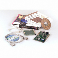
KIT EZ-USB DEVELOPMENT BOARD
Manufacturer
Cypress Semiconductor Corp
Datasheet
1.AN2131SC.pdf
(334 pages)
Specifications of AN2131-DK001
Lead Free Status / RoHS Status
Contains lead / RoHS non-compliant
Other names
428-1333


The EZ-USB chip has three resets:
This chapter describes the effects of these three resets.
When power is first applied to the EZ-USB chip, the external R-C circuit holds the EZ-
USB core in reset until the on-chip PLL stabilizes. The CLK24 pin is active as soon as
power is applied. The 8051 may clear an EZ-USB control bit, CLK24OE, to inhibit the
CLK24 output pin for EMI-sensitive applications that do not need this signal. External
logic can force a chip reset by pulling the RESET pin HI. The RESET pin is normally
EZ-USB TRM v1.9
10.1
10.2
•
•
•
A Power-On Reset (POR), which turns on the EZ-USB chip in a known state.
An 8051 reset, controlled by the EZ-USB core.
A USB bus reset, sent by the host to reset a device.
Introduction
EZ-USB Power-On Reset (POR)
MHz
12
Vcc
XOUT
RESET
XIN
10 EZ-USB Resets
Figure 10-1. EZ-USB Resets
Chapter 10. EZ-USB Resets
Oscillator
RES
USB Bus
Reset
EZ-USB Core
(1 at PWR ON)
PLL
CPUCS.0
48 MHz
RES
8051
÷2
24 MHz
CLK24
Page 10-1
Related parts for AN2131-DK001
Image
Part Number
Description
Manufacturer
Datasheet
Request
R

Part Number:
Description:
Two Chip Voltage Controlled Amplifier & Video Switch
Manufacturer:
Analog Devices

Part Number:
Description:
Manufacturer:
Cypress Semiconductor Corp
Datasheet:
Part Number:
Description:
Manufacturer:
Cypress Semiconductor Corp
Datasheet:
Part Number:
Description:
Manufacturer:
Cypress Semiconductor Corp
Datasheet:
Part Number:
Description:
Manufacturer:
Cypress Semiconductor Corp
Datasheet:
Part Number:
Description:
Manufacturer:
Cypress Semiconductor Corp
Datasheet: