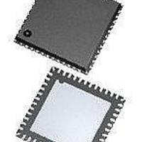
MC9S08JM16CGT Freescale Semiconductor, MC9S08JM16CGT Datasheet - Page 246

MC9S08JM16CGT
Manufacturer Part Number
MC9S08JM16CGT
Description
MCU 8BIT 16K FLASH 48-QFN
Manufacturer
Freescale Semiconductor
Series
HCS08r
Datasheet
1.DEMO9S08JM16.pdf
(386 pages)
Specifications of MC9S08JM16CGT
Core Processor
HCS08
Core Size
8-Bit
Speed
48MHz
Connectivity
I²C, LIN, SCI, SPI, USB
Peripherals
LVD, POR, PWM, WDT
Number Of I /o
37
Program Memory Size
16KB (16K x 8)
Program Memory Type
FLASH
Ram Size
1K x 8
Voltage - Supply (vcc/vdd)
2.7 V ~ 5.5 V
Data Converters
A/D 8x12b
Oscillator Type
External
Operating Temperature
-40°C ~ 85°C
Package / Case
48-QFN Exposed Pad
Processor Series
S08JM
Core
HCS08
Data Bus Width
8 bit
Data Ram Size
1 KB
Interface Type
I2C, SPI
Maximum Clock Frequency
48 MHz
Number Of Programmable I/os
37
Number Of Timers
2
Operating Supply Voltage
2.7 V to 5.5 V
Maximum Operating Temperature
+ 85 C
Mounting Style
SMD/SMT
3rd Party Development Tools
EWS08
Development Tools By Supplier
DEMOJM, DEMOJMSKT, DEMOFLEXISJMSD, DEMO9S08JM16
Minimum Operating Temperature
- 40 C
On-chip Adc
12 bit, 8 Channel
Controller Family/series
HCS08
No. Of I/o's
37
Ram Memory Size
1KB
Cpu Speed
48MHz
No. Of Timers
2
Digital Ic Case Style
QFN
Rohs Compliant
Yes
Lead Free Status / RoHS Status
Lead free / RoHS Compliant
Eeprom Size
-
Lead Free Status / Rohs Status
Lead free / RoHS Compliant
Available stocks
Company
Part Number
Manufacturer
Quantity
Price
Company:
Part Number:
MC9S08JM16CGT
Manufacturer:
PIXART
Quantity:
1 001
Part Number:
MC9S08JM16CGT
Manufacturer:
FREESCALE
Quantity:
20 000
- Current page: 246 of 386
- Download datasheet (8Mb)
Serial Peripheral Interface (S08SPI16V1)
15.3.2
This read/write register is used to control optional features of the SPI system. Bits 6 and 5 are not
implemented and always read 0.
246
LSBFE
SPTIE
MSTR
CPHA
SSOE
CPOL
Field
SPIE
SPE
7
6
5
4
3
2
1
0
SPI Control Register 2 (SPIxC2)
SPI Interrupt Enable (for SPRF and MODF) — This is the interrupt enable for SPI receive buffer full (SPRF)
and mode fault (MODF) events.
0 Interrupts from SPRF and MODF inhibited (use polling)
1 When SPRF or MODF is 1, request a hardware interrupt
SPI System Enable — This bit enables the SPI system and dedicates the SPI port pins to SPI system functions.
If SPE is cleared, SPI is disabled and forced into idle state, and all status bits in the SPIxS register are reset.
0 SPI system inactive
1 SPI system enabled
SPI Transmit Interrupt Enable — This is the interrupt enable bit for SPI transmit buffer empty (SPTEF).
0 Interrupts from SPTEF inhibited (use polling)
1 When SPTEF is 1, hardware interrupt requested
Master/Slave Mode Select — This bit selects master or slave mode operation.
0 SPI module configured as a slave SPI device
1 SPI module configured as a master SPI device
Clock Polarity — This bit selects an inverted or non-inverted SPI clock. To transmit data between SPI modules,
the SPI modules must have identical CPOL values.
This bit effectively places an inverter in series with the clock signal from a master SPI or to a slave SPI device.
Refer to
0 Active-high SPI clock (idles low)
1 Active-low SPI clock (idles high)
Clock Phase — This bit selects one of two clock formats for different kinds of synchronous serial peripheral
devices. Refer to
0 First edge on SPSCK occurs at the middle of the first cycle of a data transfer
1 First edge on SPSCK occurs at the start of the first cycle of a data transfer
Slave Select Output Enable — This bit is used in combination with the mode fault enable (MODFEN) bit in
SPIxC2 and the master/slave (MSTR) control bit to determine the function of the SS pin as shown in
LSB First (Shifter Direction) — This bit does not affect the position of the MSB and LSB in the data register.
Reads and writes of the data register always have the MSB in bit 7 (or bit 15 in 16-bit mode).
0 SPI serial data transfers start with most significant bit
1 SPI serial data transfers start with least significant bit
MODFEN
0
0
1
1
Section 15.4.5, “SPI Clock
Section 15.4.5, “SPI Clock
SSOE
0
1
0
1
Table 15-1. SPIxC1 Field Descriptions
MC9S08JM16 Series Data Sheet, Rev. 2
Table 15-2. SS Pin Function
General-purpose I/O (not SPI)
General-purpose I/O (not SPI)
SS input for mode fault
Automatic SS output
Formats”
Master Mode
Formats”
for more details.
Description
for more details.
Slave select input
Slave select input
Slave select input
Slave select input
Slave Mode
Freescale Semiconductor
Table
15-2.
Related parts for MC9S08JM16CGT
Image
Part Number
Description
Manufacturer
Datasheet
Request
R
Part Number:
Description:
Manufacturer:
Freescale Semiconductor, Inc
Datasheet:
Part Number:
Description:
Manufacturer:
Freescale Semiconductor, Inc
Datasheet:
Part Number:
Description:
Manufacturer:
Freescale Semiconductor, Inc
Datasheet:
Part Number:
Description:
Manufacturer:
Freescale Semiconductor, Inc
Datasheet:
Part Number:
Description:
Manufacturer:
Freescale Semiconductor, Inc
Datasheet:
Part Number:
Description:
Manufacturer:
Freescale Semiconductor, Inc
Datasheet:
Part Number:
Description:
Manufacturer:
Freescale Semiconductor, Inc
Datasheet:
Part Number:
Description:
Manufacturer:
Freescale Semiconductor, Inc
Datasheet:
Part Number:
Description:
Manufacturer:
Freescale Semiconductor, Inc
Datasheet:
Part Number:
Description:
Manufacturer:
Freescale Semiconductor, Inc
Datasheet:
Part Number:
Description:
Manufacturer:
Freescale Semiconductor, Inc
Datasheet:
Part Number:
Description:
Manufacturer:
Freescale Semiconductor, Inc
Datasheet:
Part Number:
Description:
Manufacturer:
Freescale Semiconductor, Inc
Datasheet:
Part Number:
Description:
Manufacturer:
Freescale Semiconductor, Inc
Datasheet:
Part Number:
Description:
Manufacturer:
Freescale Semiconductor, Inc
Datasheet:


