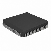
PIC17LC752T-08I/L Microchip Technology, PIC17LC752T-08I/L Datasheet - Page 143

PIC17LC752T-08I/L
Manufacturer Part Number
PIC17LC752T-08I/L
Description
IC MCU OTP 8KX16 A/D 68PLCC
Manufacturer
Microchip Technology
Series
PIC® 17Cr
Specifications of PIC17LC752T-08I/L
Core Processor
PIC
Core Size
8-Bit
Speed
8MHz
Connectivity
I²C, SPI, UART/USART
Peripherals
Brown-out Detect/Reset, POR, PWM, WDT
Number Of I /o
50
Program Memory Size
16KB (8K x 16)
Program Memory Type
OTP
Ram Size
678 x 8
Voltage - Supply (vcc/vdd)
3 V ~ 5.5 V
Data Converters
A/D 12x10b
Oscillator Type
External
Operating Temperature
-40°C ~ 85°C
Package / Case
68-PLCC
Processor Series
PIC17LC
Core
PIC
Data Bus Width
8 bit
Data Ram Size
678 B
Interface Type
I2C, MSSP, RS- 232, SCI, SPI, USART
Maximum Clock Frequency
8 MHz
Number Of Programmable I/os
50
Number Of Timers
8
Operating Supply Voltage
3 V to 5.5 V
Maximum Operating Temperature
+ 85 C
Mounting Style
SMD/SMT
Development Tools By Supplier
ICE2000, DM173001
Minimum Operating Temperature
- 40 C
On-chip Adc
12 bit
Lead Free Status / RoHS Status
Lead free / RoHS Compliant
Eeprom Size
-
Lead Free Status / Rohs Status
Details
Available stocks
Company
Part Number
Manufacturer
Quantity
Price
Company:
Part Number:
PIC17LC752T-08I/L
Manufacturer:
Microchip Technology
Quantity:
10 000
- Current page: 143 of 304
- Download datasheet (6Mb)
15.2
The MSSP module in I
master and slave functions (including general call sup-
port) and provides interrupts on START and STOP bits
in hardware to determine a free bus (multi-master func-
tion). The MSSP module implements the standard
mode specifications as well as 7-bit and 10-bit
addressing.
Refer to Application Note AN578, “Use of the SSP
Module in the I
A “glitch” filter is on the SCL and SDA pins when the pin
is an input. This filter operates in both the 100 kHz and
400 kHz modes. In the 100 kHz mode, when these pins
are an output, there is a slew rate control of the pin that
is independent of device frequency.
FIGURE 15-10:
2000 Microchip Technology Inc.
SDA
SCL
MSSP I
2
Read
Clock
C Multi-Master Environment.”
Shift
2
C Operation
MSb
STOP bit Detect
I
DIAGRAM
2
Match Detect
SSPADD reg
SSPBUF reg
START and
SSPSR reg
2
C SLAVE MODE BLOCK
C mode fully implements all
LSb
Write
(SSPSTAT reg)
Data Bus
Internal
Set, Reset
S, P bits
Addr Match
FIGURE 15-11:
Two pins are used for data transfer. These are the SCL
pin, which is the clock and the SDA pin, which is the
data. The SDA and SCL pins are automatically config-
ured when the I
functions are enabled by setting SSP Enable bit
SSPEN (SSPCON1<5>).
The MSSP module has six registers for I
These are the:
• SSP Control Register1 (SSPCON1)
• SSP Control Register2 (SSPCON2)
• SSP Status Register (SSPSTAT)
• Serial Receive/Transmit Buffer (SSPBUF)
• SSP Shift Register (SSPSR) - Not directly acces-
• SSP Address Register (SSPADD)
The SSPCON1 register allows control of the I
ation. Four mode selection bits (SSPCON1<3:0>) allow
one of the following I
• I
• I
• I
Before selecting any I
must be programmed to inputs by setting the appropri-
ate DDR bits. Selecting an I
SSPEN bit, enables the SCL and SDA pins to be used
as the clock and data lines in I
sible
SDA
SCL
Baud Rate Generator
2
2
2
SSPADD<6:0>
C Slave mode (7-bit address)
C Slave mode (10-bit address)
C Master mode, clock = OSC/4 (SSPADD +1)
7
Read
2
Clock
Shift
C mode is enabled. The SSP module
MSb
START and STOP bit
2
C modes to be selected:
2
I
BLOCK DIAGRAM
Detect/Generate
C mode, the SCL and SDA pins
2
Match Detect
SSPADD reg
SSPBUF reg
SSPSR reg
PIC17C7XX
C MASTER MODE
2
2
C mode, by setting the
C mode.
LSb
DS30289B-page 143
Write
(SSPSTAT reg)
Clear/Set P, bit
and Set SSPIF
Set/Clear S bit
Data Bus
2
Internal
C operation.
Addr Match
and
2
C oper-
Related parts for PIC17LC752T-08I/L
Image
Part Number
Description
Manufacturer
Datasheet
Request
R

Part Number:
Description:
IC MCU OTP 8KX16 A/D 68PLCC
Manufacturer:
Microchip Technology
Datasheet:

Part Number:
Description:
IC MCU OTP 8KX16 A/D 68PLCC
Manufacturer:
Microchip Technology
Datasheet:

Part Number:
Description:
IC MCU OTP 8KX16 A/D 64TQFP
Manufacturer:
Microchip Technology
Datasheet:

Part Number:
Description:
IC MCU OTP 8KX16 A/D 64TQFP
Manufacturer:
Microchip Technology
Datasheet:

Part Number:
Description:
Manufacturer:
Microchip Technology Inc.
Datasheet:

Part Number:
Description:
Manufacturer:
Microchip Technology Inc.
Datasheet:

Part Number:
Description:
Manufacturer:
Microchip Technology Inc.
Datasheet:

Part Number:
Description:
Manufacturer:
Microchip Technology Inc.
Datasheet:

Part Number:
Description:
Manufacturer:
Microchip Technology Inc.
Datasheet:

Part Number:
Description:
Manufacturer:
Microchip Technology Inc.
Datasheet:

Part Number:
Description:
Manufacturer:
Microchip Technology Inc.
Datasheet:


