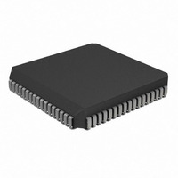
PIC17LC752T-08I/L Microchip Technology, PIC17LC752T-08I/L Datasheet - Page 153

PIC17LC752T-08I/L
Manufacturer Part Number
PIC17LC752T-08I/L
Description
IC MCU OTP 8KX16 A/D 68PLCC
Manufacturer
Microchip Technology
Series
PIC® 17Cr
Specifications of PIC17LC752T-08I/L
Core Processor
PIC
Core Size
8-Bit
Speed
8MHz
Connectivity
I²C, SPI, UART/USART
Peripherals
Brown-out Detect/Reset, POR, PWM, WDT
Number Of I /o
50
Program Memory Size
16KB (8K x 16)
Program Memory Type
OTP
Ram Size
678 x 8
Voltage - Supply (vcc/vdd)
3 V ~ 5.5 V
Data Converters
A/D 12x10b
Oscillator Type
External
Operating Temperature
-40°C ~ 85°C
Package / Case
68-PLCC
Processor Series
PIC17LC
Core
PIC
Data Bus Width
8 bit
Data Ram Size
678 B
Interface Type
I2C, MSSP, RS- 232, SCI, SPI, USART
Maximum Clock Frequency
8 MHz
Number Of Programmable I/os
50
Number Of Timers
8
Operating Supply Voltage
3 V to 5.5 V
Maximum Operating Temperature
+ 85 C
Mounting Style
SMD/SMT
Development Tools By Supplier
ICE2000, DM173001
Minimum Operating Temperature
- 40 C
On-chip Adc
12 bit
Lead Free Status / RoHS Status
Lead free / RoHS Compliant
Eeprom Size
-
Lead Free Status / Rohs Status
Details
Available stocks
Company
Part Number
Manufacturer
Quantity
Price
Company:
Part Number:
PIC17LC752T-08I/L
Manufacturer:
Microchip Technology
Quantity:
10 000
- Current page: 153 of 304
- Download datasheet (6Mb)
A typical transmit sequence would go as follows:
a)
b)
c)
d)
e)
f)
g)
h)
i)
j)
k)
l)
FIGURE 15-19:
2000 Microchip Technology Inc.
The user generates a START Condition by set-
ting the START enable bit (SEN) in SSPCON2.
SSPIF is set. The module will wait the required
START time before any other operation takes
place.
The user loads the SSPBUF with address to
transmit.
Address is shifted out the SDA pin until all 8 bits
are transmitted.
The MSSP Module shifts in the ACK bit from the
slave device and writes its value into the
SSPCON2 register (SSPCON2<6>).
The module generates an interrupt at the end of
the ninth clock cycle by setting SSPIF.
The user loads the SSPBUF with eight bits of data.
DATA is shifted out the SDA pin until all 8 bits are
transmitted.
The MSSP Module shifts in the ACK bit from the
slave device, and writes its value into the
SSPCON2 register (SSPCON2<6>).
The MSSP module generates an interrupt at the
end of the ninth clock cycle by setting the SSPIF
bit.
The user generates a STOP condition by setting
the STOP enable bit PEN in SSPCON2.
Interrupt is generated once the STOP condition
is complete.
SDA
SCL
BRG
Value
BRG
Reload
BAUD RATE GENERATOR TIMING WITH CLOCK ARBITRATION
03h
DX
SCL de-asserted but slave holds
SCL low (clock arbitration).
02h
SCL is sampled high, reload takes
place and BRG starts its count.
01h
BRG decrements
(on Q2 and Q4 cycles).
00h (hold off)
DX-1
15.2.8
In I
located in the lower 7 bits of the SSPADD register
(Figure 15-18). When the BRG is loaded with this
value, the BRG counts down to 0 and stops until
another reload has taken place. The BRG count is dec-
remented twice per instruction cycle (T
and Q4 clock.
In I
If Clock Arbitration is taking place, for instance, the
BRG will be reloaded when the SCL pin is sampled
high (Figure 15-19).
FIGURE 15-18:
SSPM3:SSPM0
2
2
SSPM3:SSPM0
C Master mode, the BRG is reloaded automatically.
C Master mode, the reload value for the BRG is
SCL
BAUD RATE GENERATOR
SCL allowed to transition high.
CLKOUT
03h
BAUD RATE GENERATOR
BLOCK DIAGRAM
PIC17C7XX
Reload
Control
02h
BRG Down Counter
SSPADD<6:0>
Reload
DS30289B-page 153
CY
), on the Q2
F
OSC
/4
Related parts for PIC17LC752T-08I/L
Image
Part Number
Description
Manufacturer
Datasheet
Request
R

Part Number:
Description:
IC MCU OTP 8KX16 A/D 68PLCC
Manufacturer:
Microchip Technology
Datasheet:

Part Number:
Description:
IC MCU OTP 8KX16 A/D 68PLCC
Manufacturer:
Microchip Technology
Datasheet:

Part Number:
Description:
IC MCU OTP 8KX16 A/D 64TQFP
Manufacturer:
Microchip Technology
Datasheet:

Part Number:
Description:
IC MCU OTP 8KX16 A/D 64TQFP
Manufacturer:
Microchip Technology
Datasheet:

Part Number:
Description:
Manufacturer:
Microchip Technology Inc.
Datasheet:

Part Number:
Description:
Manufacturer:
Microchip Technology Inc.
Datasheet:

Part Number:
Description:
Manufacturer:
Microchip Technology Inc.
Datasheet:

Part Number:
Description:
Manufacturer:
Microchip Technology Inc.
Datasheet:

Part Number:
Description:
Manufacturer:
Microchip Technology Inc.
Datasheet:

Part Number:
Description:
Manufacturer:
Microchip Technology Inc.
Datasheet:

Part Number:
Description:
Manufacturer:
Microchip Technology Inc.
Datasheet:


