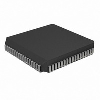
PIC17LC752T-08I/L Microchip Technology, PIC17LC752T-08I/L Datasheet - Page 51

PIC17LC752T-08I/L
Manufacturer Part Number
PIC17LC752T-08I/L
Description
IC MCU OTP 8KX16 A/D 68PLCC
Manufacturer
Microchip Technology
Series
PIC® 17Cr
Specifications of PIC17LC752T-08I/L
Core Processor
PIC
Core Size
8-Bit
Speed
8MHz
Connectivity
I²C, SPI, UART/USART
Peripherals
Brown-out Detect/Reset, POR, PWM, WDT
Number Of I /o
50
Program Memory Size
16KB (8K x 16)
Program Memory Type
OTP
Ram Size
678 x 8
Voltage - Supply (vcc/vdd)
3 V ~ 5.5 V
Data Converters
A/D 12x10b
Oscillator Type
External
Operating Temperature
-40°C ~ 85°C
Package / Case
68-PLCC
Processor Series
PIC17LC
Core
PIC
Data Bus Width
8 bit
Data Ram Size
678 B
Interface Type
I2C, MSSP, RS- 232, SCI, SPI, USART
Maximum Clock Frequency
8 MHz
Number Of Programmable I/os
50
Number Of Timers
8
Operating Supply Voltage
3 V to 5.5 V
Maximum Operating Temperature
+ 85 C
Mounting Style
SMD/SMT
Development Tools By Supplier
ICE2000, DM173001
Minimum Operating Temperature
- 40 C
On-chip Adc
12 bit
Lead Free Status / RoHS Status
Lead free / RoHS Compliant
Eeprom Size
-
Lead Free Status / Rohs Status
Details
Available stocks
Company
Part Number
Manufacturer
Quantity
Price
Company:
Part Number:
PIC17LC752T-08I/L
Manufacturer:
Microchip Technology
Quantity:
10 000
- Current page: 51 of 304
- Download datasheet (6Mb)
7.2.2.1
The ALUSTA register contains the status bits of the
Arithmetic and Logic Unit and the mode control bits for
the indirect addressing register.
As with all the other registers, the ALUSTA register can
be the destination for any instruction. If the ALUSTA
register is the destination for an instruction that affects
the Z, DC, C, or OV bits, then the write to these three
bits is disabled. These bits are set or cleared according
to the device logic. Therefore, the result of an instruc-
tion with the ALUSTA register as destination may be
different than intended.
For example, the CLRF ALUSTA, F instruction will clear
the upper four bits and set the Z bit. This leaves the
ALUSTA register as 0000u1uu (where u = unchanged).
REGISTER 7-1: ALUSTA REGISTER (ADDRESS: 04h, UNBANKED)
2000 Microchip Technology Inc.
bit 7-6
bit 5-4
bit 3
bit 2
bit 1
bit 0
ALU Status Register (ALUSTA)
Legend:
R = Readable bit
- n = Value at POR Reset
bit 7
FS3:FS2: FSR1 Mode Select bits
00 = Post auto-decrement FSR1 value
01 = Post auto-increment FSR1 value
1x = FSR1 value does not change
FS1:FS0: FSR0 Mode Select bits
00 = Post auto-decrement FSR0 value
01 = Post auto-increment FSR0 value
1x = FSR0 value does not change
OV: Overflow bit
This bit is used for signed arithmetic (2’s complement). It indicates an overflow of the 7-bit
magnitude, which causes the sign bit (bit7) to change state.
1 = Overflow occurred for signed arithmetic (in this arithmetic operation)
0 = No overflow occurred
Z: Zero bit
1 = The result of an arithmetic or logic operation is zero
0 = The result of an arithmetic or logic operation is not zero
DC: Digit carry/borrow bit
For ADDWF and ADDLW instructions.
1 = A carry-out from the 4th low order bit of the result occurred
0 = No carry-out from the 4th low order bit of the result
C: Carry/borrow bit
For ADDWF and ADDLW instructions. Note that a subtraction is executed by adding the two’s
complement of the second operand.
For rotate (RRCF, RLCF) instructions, this bit is loaded with either the high or low order bit of the
source register.
1 = A carry-out from the Most Significant bit of the result occurred
0 = No carry-out from the Most Significant bit of the result
R/W-1
Note:
Note:
FS3
For borrow, the polarity is reversed.
For borrow, the polarity is reversed.
R/W-1
FS2
R/W-1
FS1
W = Writable bit
’1’ = Bit is set
R/W-1
FS0
It is recommended, therefore, that only BCF, BSF, SWAPF
and MOVWF instructions be used to alter the ALUSTA
register, because these instructions do not affect any
status bits. To see how other instructions affect the sta-
tus bits, see the “Instruction Set Summary.”
The Arithmetic and Logic Unit (ALU) is capable of car-
rying out arithmetic or logical operations on two oper-
ands, or a single operand. All single operand
instructions operate either on the WREG register, or
the given file register. For two operand instructions, one
of the operands is the WREG register and the other is
either a file register, or an 8-bit immediate constant.
Note 1: The C and DC bits operate as a borrow and
2: The overflow bit will be set if the 2’s comple-
R/W-x
U = Unimplemented bit, read as ‘0’
’0’ = Bit is cleared
OV
ment result exceeds +127, or is less than -128.
digit borrow bit, respectively, in subtraction.
See the SUBLW and SUBWF instructions for
examples.
R/W-x
PIC17C7XX
Z
x = Bit is unknown
R/W-x
DC
DS30289B-page 51
R/W-x
C
bit 0
Related parts for PIC17LC752T-08I/L
Image
Part Number
Description
Manufacturer
Datasheet
Request
R

Part Number:
Description:
IC MCU OTP 8KX16 A/D 68PLCC
Manufacturer:
Microchip Technology
Datasheet:

Part Number:
Description:
IC MCU OTP 8KX16 A/D 68PLCC
Manufacturer:
Microchip Technology
Datasheet:

Part Number:
Description:
IC MCU OTP 8KX16 A/D 64TQFP
Manufacturer:
Microchip Technology
Datasheet:

Part Number:
Description:
IC MCU OTP 8KX16 A/D 64TQFP
Manufacturer:
Microchip Technology
Datasheet:

Part Number:
Description:
Manufacturer:
Microchip Technology Inc.
Datasheet:

Part Number:
Description:
Manufacturer:
Microchip Technology Inc.
Datasheet:

Part Number:
Description:
Manufacturer:
Microchip Technology Inc.
Datasheet:

Part Number:
Description:
Manufacturer:
Microchip Technology Inc.
Datasheet:

Part Number:
Description:
Manufacturer:
Microchip Technology Inc.
Datasheet:

Part Number:
Description:
Manufacturer:
Microchip Technology Inc.
Datasheet:

Part Number:
Description:
Manufacturer:
Microchip Technology Inc.
Datasheet:


