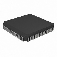
PIC17LC752T-08I/L Microchip Technology, PIC17LC752T-08I/L Datasheet - Page 239

PIC17LC752T-08I/L
Manufacturer Part Number
PIC17LC752T-08I/L
Description
IC MCU OTP 8KX16 A/D 68PLCC
Manufacturer
Microchip Technology
Series
PIC® 17Cr
Specifications of PIC17LC752T-08I/L
Core Processor
PIC
Core Size
8-Bit
Speed
8MHz
Connectivity
I²C, SPI, UART/USART
Peripherals
Brown-out Detect/Reset, POR, PWM, WDT
Number Of I /o
50
Program Memory Size
16KB (8K x 16)
Program Memory Type
OTP
Ram Size
678 x 8
Voltage - Supply (vcc/vdd)
3 V ~ 5.5 V
Data Converters
A/D 12x10b
Oscillator Type
External
Operating Temperature
-40°C ~ 85°C
Package / Case
68-PLCC
Processor Series
PIC17LC
Core
PIC
Data Bus Width
8 bit
Data Ram Size
678 B
Interface Type
I2C, MSSP, RS- 232, SCI, SPI, USART
Maximum Clock Frequency
8 MHz
Number Of Programmable I/os
50
Number Of Timers
8
Operating Supply Voltage
3 V to 5.5 V
Maximum Operating Temperature
+ 85 C
Mounting Style
SMD/SMT
Development Tools By Supplier
ICE2000, DM173001
Minimum Operating Temperature
- 40 C
On-chip Adc
12 bit
Lead Free Status / RoHS Status
Lead free / RoHS Compliant
Eeprom Size
-
Lead Free Status / Rohs Status
Details
Available stocks
Company
Part Number
Manufacturer
Quantity
Price
Company:
Part Number:
PIC17LC752T-08I/L
Manufacturer:
Microchip Technology
Quantity:
10 000
- Current page: 239 of 304
- Download datasheet (6Mb)
20.0
Absolute Maximum Ratings †
Ambient temperature under bias.............................................................................................................-55°C to +125°C
Storage temperature .............................................................................................................................. -65°C to +150°C
Voltage on V
Voltage on MCLR with respect to V
Voltage on RA2 and RA3 with respect to V
Voltage on all other pins with respect to V
Total power dissipation (Note 1) ..............................................................................................................................1.0 W
Maximum current out of V
Maximum current into V
Input clamp current, I
Output clamp current, I
Maximum output current sunk by any I/O pin (except RA2 and RA3).....................................................................35 mA
Maximum output current sunk by RA2 or RA3 pins ................................................................................................60 mA
Maximum output current sourced by any I/O pin ....................................................................................................20 mA
Maximum current sunk by PORTA and PORTB (combined).................................................................................150 mA
Maximum current sourced by PORTA and PORTB (combined) ...........................................................................100 mA
Maximum current sunk by PORTC, PORTD and PORTE (combined)..................................................................150 mA
Maximum current sourced by PORTC, PORTD and PORTE (combined) ............................................................100 mA
Maximum current sunk by PORTF and PORTG (combined) ................................................................................150 mA
Maximum current sourced by PORTF and PORTG (combined)...........................................................................100 mA
Maximum current sunk by PORTH and PORTJ (combined).................................................................................150 mA
Maximum current sourced by PORTH and PORTJ (combined) ...........................................................................100 mA
† NOTICE: Stresses above those listed under "Absolute Maximum Ratings" may cause permanent dam-
age to the device. This is a stress rating only and functional operation of the device at those or any other
conditions above those indicated in the operation listings of this specification is not implied. Exposure to
maximum rating conditions for extended periods may affect device reliability.
2000 Microchip Technology Inc.
Note 1: Power dissipation is calculated as follows: Pdis = V
2: Voltage spikes below V
PIC17C7XX ELECTRICAL CHARACTERISTICS
Thus, a series resistor of 50-100
pulling this pin directly to V
DD
with respect to V
IK
OK
(V
DD
SS
I
(V
< 0 or V
pin(s) - total (@ 70°C) ...............................................................................................500 mA
O
pin(s) - total (@ 70°C) ............................................................................................500 mA
< 0 or V
SS
I
SS
SS
> V
........................................................................................................... 0 V to +7.5 V
O
SS
(Note 2) ....................................................................................... -0.3 V to +14 V
at the MCLR pin, inducing currents greater than 80 mA, may cause latch-up.
DD
> V
.
SS
) .......................................................................................................... ±20 mA
SS
DD
...................................................................................-0.3 V to V
.......................................................................................... -0.3 V to +8.5 V
) ...................................................................................................±20 mA
should be used when applying a "low" level to the MCLR pin, rather than
DD
x {I
DD
-
I
OH
} +
{(V
PIC17C7XX
DD
-V
OH
) x I
DS30289B-page 239
OH
} + (V
DD
OL
+ 0.3 V
x I
OL
)
Related parts for PIC17LC752T-08I/L
Image
Part Number
Description
Manufacturer
Datasheet
Request
R

Part Number:
Description:
IC MCU OTP 8KX16 A/D 68PLCC
Manufacturer:
Microchip Technology
Datasheet:

Part Number:
Description:
IC MCU OTP 8KX16 A/D 68PLCC
Manufacturer:
Microchip Technology
Datasheet:

Part Number:
Description:
IC MCU OTP 8KX16 A/D 64TQFP
Manufacturer:
Microchip Technology
Datasheet:

Part Number:
Description:
IC MCU OTP 8KX16 A/D 64TQFP
Manufacturer:
Microchip Technology
Datasheet:

Part Number:
Description:
Manufacturer:
Microchip Technology Inc.
Datasheet:

Part Number:
Description:
Manufacturer:
Microchip Technology Inc.
Datasheet:

Part Number:
Description:
Manufacturer:
Microchip Technology Inc.
Datasheet:

Part Number:
Description:
Manufacturer:
Microchip Technology Inc.
Datasheet:

Part Number:
Description:
Manufacturer:
Microchip Technology Inc.
Datasheet:

Part Number:
Description:
Manufacturer:
Microchip Technology Inc.
Datasheet:

Part Number:
Description:
Manufacturer:
Microchip Technology Inc.
Datasheet:


