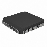
PIC17LC752T-08I/L Microchip Technology, PIC17LC752T-08I/L Datasheet - Page 194

PIC17LC752T-08I/L
Manufacturer Part Number
PIC17LC752T-08I/L
Description
IC MCU OTP 8KX16 A/D 68PLCC
Manufacturer
Microchip Technology
Series
PIC® 17Cr
Specifications of PIC17LC752T-08I/L
Core Processor
PIC
Core Size
8-Bit
Speed
8MHz
Connectivity
I²C, SPI, UART/USART
Peripherals
Brown-out Detect/Reset, POR, PWM, WDT
Number Of I /o
50
Program Memory Size
16KB (8K x 16)
Program Memory Type
OTP
Ram Size
678 x 8
Voltage - Supply (vcc/vdd)
3 V ~ 5.5 V
Data Converters
A/D 12x10b
Oscillator Type
External
Operating Temperature
-40°C ~ 85°C
Package / Case
68-PLCC
Processor Series
PIC17LC
Core
PIC
Data Bus Width
8 bit
Data Ram Size
678 B
Interface Type
I2C, MSSP, RS- 232, SCI, SPI, USART
Maximum Clock Frequency
8 MHz
Number Of Programmable I/os
50
Number Of Timers
8
Operating Supply Voltage
3 V to 5.5 V
Maximum Operating Temperature
+ 85 C
Mounting Style
SMD/SMT
Development Tools By Supplier
ICE2000, DM173001
Minimum Operating Temperature
- 40 C
On-chip Adc
12 bit
Lead Free Status / RoHS Status
Lead free / RoHS Compliant
Eeprom Size
-
Lead Free Status / Rohs Status
Details
Available stocks
Company
Part Number
Manufacturer
Quantity
Price
Company:
Part Number:
PIC17LC752T-08I/L
Manufacturer:
Microchip Technology
Quantity:
10 000
- Current page: 194 of 304
- Download datasheet (6Mb)
PIC17C7XX
17.4
The Power-down mode is entered by executing a
SLEEP instruction. This clears the Watchdog Timer and
postscaler (if enabled). The PD bit is cleared and the
TO bit is set (in the CPUSTA register). In SLEEP mode,
the oscillator driver is turned off. The I/O ports maintain
their status (driving high,low, or hi-impedance input).
The MCLR/V
(V
MCLR/V
17.4.1
The device can wake-up from SLEEP through one of
the following events:
• Power-on Reset
• Brown-out Reset
• External RESET input on MCLR/V
• WDT Reset (if WDT was enabled)
• Interrupt from RA0/INT pin, RB port change,
The following peripheral interrupts can wake the device
from SLEEP:
• Capture interrupts
• USART synchronous slave transmit interrupts
• USART synchronous slave receive interrupts
• A/D conversion complete
• SPI slave transmit/receive complete
• I
Other peripherals cannot generate interrupts since dur-
ing SLEEP, no on-chip Q clocks are present.
FIGURE 17-2:
DS30289B-page 194
(RA0/INT pin)
IHMC
T0CKI interrupt, or some peripheral interrupts
INSTRUCTION FLOW
2
Note 1: XT or LF oscillator mode assumed.
CLKOUT
GLINTD bit
C slave receive
Instruction
Executed
INTF Flag
Instruction
Fetched
PC
). A WDT time-out RESET does not drive the
2: T
3: When GLINTD = 0, processor jumps to interrupt routine after wake-up. If GLINTD = 1, execution will continue in line.
4: CLKOUT is not available in these osc modes, but shown here for timing reference.
OSC1
PP
Power-down Mode (SLEEP)
INT
OST
pin low.
WAKE-UP FROM SLEEP
(4)
PP
= 1024T
pin must be at a logic high level
’0’ or ’1’
Inst (PC) = SLEEP
Q1
Inst (PC-1)
OSC
WAKE-UP FROM SLEEP THROUGH INTERRUPT
Q2
PC
(drawing not to scale). This delay will not be there for RC osc mode.
Q3
Q4
PP
Q1
pin
Inst (PC+1)
SLEEP
Q2
PC+1
Q3
Q4
Processor
in SLEEP
Q1
Q2
Any RESET event will cause a device RESET. Any
interrupt event is considered a continuation of program
execution. The TO and PD bits in the CPUSTA register
can be used to determine the cause of a device
RESET. The PD bit, which is set on power-up, is
cleared when SLEEP is invoked. The TO bit is cleared
if WDT time-out occurred (and caused a RESET).
When the SLEEP instruction is being executed, the next
instruction (PC + 1) is pre-fetched. For the device to
wake-up through an interrupt event, the corresponding
interrupt enable bit must be set (enabled). Wake-up is
regardless of the state of the GLINTD bit. If the GLINTD
bit is set (disabled), the device continues execution at
the instruction after the SLEEP instruction. If the
GLINTD bit is clear (enabled), the device executes the
instruction after the SLEEP instruction and then
branches to the interrupt vector address. In cases
where the execution of the instruction following SLEEP
is not desirable, the user should have a NOP after the
SLEEP instruction.
The WDT is cleared when the device wakes from
SLEEP, regardless of the source of wake-up.
17.4.1.1
When the oscillator type is configured in XT or LF
mode, the Oscillator Start-up Timer (OST) is activated
on wake-up. The OST will keep the device in RESET
for 1024T
when considering the interrupt response time when
coming out of SLEEP.
PC+2
Note:
Q3
T
OST
(2)
Q4
OSC
If the global interrupt is disabled (GLINTD
is set), but any interrupt source has both its
interrupt enable bit and the corresponding
interrupt flag bit set, the device will imme-
diately wake-up from SLEEP. The TO bit is
set and the PD bit is cleared.
Wake-up Delay
. This needs to be taken into account
Q1
Inst (PC+2)
Inst (PC+1)
Q2
0004h
Q3
2000 Microchip Technology Inc.
Q4
Interrupt Latency
Q1
Dummy Cycle
Q2
0005h
Q3
(2)
Q4
Related parts for PIC17LC752T-08I/L
Image
Part Number
Description
Manufacturer
Datasheet
Request
R

Part Number:
Description:
IC MCU OTP 8KX16 A/D 68PLCC
Manufacturer:
Microchip Technology
Datasheet:

Part Number:
Description:
IC MCU OTP 8KX16 A/D 68PLCC
Manufacturer:
Microchip Technology
Datasheet:

Part Number:
Description:
IC MCU OTP 8KX16 A/D 64TQFP
Manufacturer:
Microchip Technology
Datasheet:

Part Number:
Description:
IC MCU OTP 8KX16 A/D 64TQFP
Manufacturer:
Microchip Technology
Datasheet:

Part Number:
Description:
Manufacturer:
Microchip Technology Inc.
Datasheet:

Part Number:
Description:
Manufacturer:
Microchip Technology Inc.
Datasheet:

Part Number:
Description:
Manufacturer:
Microchip Technology Inc.
Datasheet:

Part Number:
Description:
Manufacturer:
Microchip Technology Inc.
Datasheet:

Part Number:
Description:
Manufacturer:
Microchip Technology Inc.
Datasheet:

Part Number:
Description:
Manufacturer:
Microchip Technology Inc.
Datasheet:

Part Number:
Description:
Manufacturer:
Microchip Technology Inc.
Datasheet:


