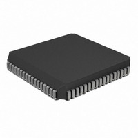
PIC17LC752T-08I/L Microchip Technology, PIC17LC752T-08I/L Datasheet - Page 53

PIC17LC752T-08I/L
Manufacturer Part Number
PIC17LC752T-08I/L
Description
IC MCU OTP 8KX16 A/D 68PLCC
Manufacturer
Microchip Technology
Series
PIC® 17Cr
Specifications of PIC17LC752T-08I/L
Core Processor
PIC
Core Size
8-Bit
Speed
8MHz
Connectivity
I²C, SPI, UART/USART
Peripherals
Brown-out Detect/Reset, POR, PWM, WDT
Number Of I /o
50
Program Memory Size
16KB (8K x 16)
Program Memory Type
OTP
Ram Size
678 x 8
Voltage - Supply (vcc/vdd)
3 V ~ 5.5 V
Data Converters
A/D 12x10b
Oscillator Type
External
Operating Temperature
-40°C ~ 85°C
Package / Case
68-PLCC
Processor Series
PIC17LC
Core
PIC
Data Bus Width
8 bit
Data Ram Size
678 B
Interface Type
I2C, MSSP, RS- 232, SCI, SPI, USART
Maximum Clock Frequency
8 MHz
Number Of Programmable I/os
50
Number Of Timers
8
Operating Supply Voltage
3 V to 5.5 V
Maximum Operating Temperature
+ 85 C
Mounting Style
SMD/SMT
Development Tools By Supplier
ICE2000, DM173001
Minimum Operating Temperature
- 40 C
On-chip Adc
12 bit
Lead Free Status / RoHS Status
Lead free / RoHS Compliant
Eeprom Size
-
Lead Free Status / Rohs Status
Details
Available stocks
Company
Part Number
Manufacturer
Quantity
Price
Company:
Part Number:
PIC17LC752T-08I/L
Manufacturer:
Microchip Technology
Quantity:
10 000
- Current page: 53 of 304
- Download datasheet (6Mb)
7.2.2.3
This register contains various control bits. Bit7
(INTEDG) is used to control the edge upon which a sig-
nal on the RA0/INT pin will set the RA0/INT interrupt
flag. The other bits configure Timer0, it’s prescaler and
clock source.
REGISTER 7-3: T0STA REGISTER (ADDRESS: 05h, UNBANKED)
2000 Microchip Technology Inc.
bit 7
bit 6
bit 5
bit 4-1
bit 0
TMR0 Status/Control Register
(T0STA)
T0PS3:T0PS0
bit 7
INTEDG: RA0/INT Pin Interrupt Edge Select bit
This bit selects the edge upon which the interrupt is detected.
1 = Rising edge of RA0/INT pin generates interrupt
0 = Falling edge of RA0/INT pin generates interrupt
T0SE: Timer0 External Clock Input Edge Select bit
This bit selects the edge upon which TMR0 will increment.
When T0CS = 0 (External Clock):
1 = Rising edge of RA1/T0CKI pin increments TMR0 and/or sets the T0CKIF bit
0 = Falling edge of RA1/T0CKI pin increments TMR0 and/or sets a T0CKIF bit
When T0CS = 1 (Internal Clock):
Don’t care
T0CS: Timer0 Clock Source Select bit
This bit selects the clock source for Timer0.
1 = Internal instruction clock cycle (T
0 = External clock input on the T0CKI pin
T0PS3:T0PS0: Timer0 Prescale Selection bits
These bits select the prescale value for Timer0.
Unimplemented: Read as ’0’
Legend:
R = Readable bit
- n = Value at POR Reset
INTEDG
R/W-0
0000
0001
0010
0011
0100
0101
0110
0111
1xxx
R/W-0
T0SE
Prescale Value
1:1
1:2
1:4
1:8
1:16
1:32
1:64
1:128
1:256
R/W-0
T0CS
W = Writable bit
’1’ = Bit is set
CY
T0PS3
R/W-0
)
T0PS2
R/W-0
U = Unimplemented bit, read as ‘0’
’0’ = Bit is cleared
T0PS1
R/W-0
PIC17C7XX
x = Bit is unknown
T0PS0
R/W-0
DS30289B-page 53
U-0
—
bit 0
Related parts for PIC17LC752T-08I/L
Image
Part Number
Description
Manufacturer
Datasheet
Request
R

Part Number:
Description:
IC MCU OTP 8KX16 A/D 68PLCC
Manufacturer:
Microchip Technology
Datasheet:

Part Number:
Description:
IC MCU OTP 8KX16 A/D 68PLCC
Manufacturer:
Microchip Technology
Datasheet:

Part Number:
Description:
IC MCU OTP 8KX16 A/D 64TQFP
Manufacturer:
Microchip Technology
Datasheet:

Part Number:
Description:
IC MCU OTP 8KX16 A/D 64TQFP
Manufacturer:
Microchip Technology
Datasheet:

Part Number:
Description:
Manufacturer:
Microchip Technology Inc.
Datasheet:

Part Number:
Description:
Manufacturer:
Microchip Technology Inc.
Datasheet:

Part Number:
Description:
Manufacturer:
Microchip Technology Inc.
Datasheet:

Part Number:
Description:
Manufacturer:
Microchip Technology Inc.
Datasheet:

Part Number:
Description:
Manufacturer:
Microchip Technology Inc.
Datasheet:

Part Number:
Description:
Manufacturer:
Microchip Technology Inc.
Datasheet:

Part Number:
Description:
Manufacturer:
Microchip Technology Inc.
Datasheet:


