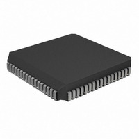
PIC17LC752T-08I/L Microchip Technology, PIC17LC752T-08I/L Datasheet - Page 82

PIC17LC752T-08I/L
Manufacturer Part Number
PIC17LC752T-08I/L
Description
IC MCU OTP 8KX16 A/D 68PLCC
Manufacturer
Microchip Technology
Series
PIC® 17Cr
Specifications of PIC17LC752T-08I/L
Core Processor
PIC
Core Size
8-Bit
Speed
8MHz
Connectivity
I²C, SPI, UART/USART
Peripherals
Brown-out Detect/Reset, POR, PWM, WDT
Number Of I /o
50
Program Memory Size
16KB (8K x 16)
Program Memory Type
OTP
Ram Size
678 x 8
Voltage - Supply (vcc/vdd)
3 V ~ 5.5 V
Data Converters
A/D 12x10b
Oscillator Type
External
Operating Temperature
-40°C ~ 85°C
Package / Case
68-PLCC
Processor Series
PIC17LC
Core
PIC
Data Bus Width
8 bit
Data Ram Size
678 B
Interface Type
I2C, MSSP, RS- 232, SCI, SPI, USART
Maximum Clock Frequency
8 MHz
Number Of Programmable I/os
50
Number Of Timers
8
Operating Supply Voltage
3 V to 5.5 V
Maximum Operating Temperature
+ 85 C
Mounting Style
SMD/SMT
Development Tools By Supplier
ICE2000, DM173001
Minimum Operating Temperature
- 40 C
On-chip Adc
12 bit
Lead Free Status / RoHS Status
Lead free / RoHS Compliant
Eeprom Size
-
Lead Free Status / Rohs Status
Details
Available stocks
Company
Part Number
Manufacturer
Quantity
Price
Company:
Part Number:
PIC17LC752T-08I/L
Manufacturer:
Microchip Technology
Quantity:
10 000
- Current page: 82 of 304
- Download datasheet (6Mb)
PIC17C7XX
10.5
PORTE is a 4-bit bi-directional port. The corresponding
data direction register is DDRE. A ’1’ in DDRE config-
ures the corresponding port pin as an input. A ’0’ in the
DDRE register configures the corresponding port pin
as an output. Reading PORTE reads the status of the
pins, whereas writing to PORTE will write to the port
latch. PORTE is multiplexed with the system bus.
When operating as the system bus, PORTE contains
the
(AD15:AD0). These control signals are Address Latch
Enable (ALE), Output Enable (OE) and Write (WR).
The control signals OE and WR are active low signals.
The timing for the system bus is shown in the Electrical
Specifications section.
FIGURE 10-11:
DS30289B-page 82
Note: I/O pins have protection diodes to V
Note:
control
PORTE and DDRE Register
Three pins of this port are configured as
the system bus when the device’s configu-
ration bits are selected to Microprocessor
or Extended Microcontroller modes. The
other pin is a general purpose I/O or
Capture4 pin. In the two other micro-
controller modes, RE2:RE0 are general
purpose I/O pins.
signals
BLOCK DIAGRAM OF RE2:RE0 (IN I/O PORT MODE)
for
TTL
Input
Buffer
the
0
1
address/data
Data
Port
DD
and V
R
Q
Q
SS
.
CK
CK
S
bus
D
D
Example 10-5 shows an instruction sequence to initial-
ize PORTE. The Bank Select Register (BSR) must be
selected to Bank 1 for the port to be initialized. The fol-
lowing example uses the MOVLB instruction to load the
BSR register for bank selection.
EXAMPLE 10-5:
MOVLB
CLRF
MOVLW
MOVWF
1
PORTE, F
0x03
DDRE
; Select Bank 1
; Initialize PORTE data
; latches before setting
; the data direction
; register
; Value used to initialize
; data direction
; Set RE<1:0> as inputs
; RE<3:2> as outputs
; RE<7:4> are always
; read as ’0’
INITIALIZING PORTE
WR_PORTE
RD_PORTE
2000 Microchip Technology Inc.
WR_DDRE
RD_DDRE
DRV_SYS
Data Bus
EX_EN
CNTL
System Bus
Control
Related parts for PIC17LC752T-08I/L
Image
Part Number
Description
Manufacturer
Datasheet
Request
R

Part Number:
Description:
IC MCU OTP 8KX16 A/D 68PLCC
Manufacturer:
Microchip Technology
Datasheet:

Part Number:
Description:
IC MCU OTP 8KX16 A/D 68PLCC
Manufacturer:
Microchip Technology
Datasheet:

Part Number:
Description:
IC MCU OTP 8KX16 A/D 64TQFP
Manufacturer:
Microchip Technology
Datasheet:

Part Number:
Description:
IC MCU OTP 8KX16 A/D 64TQFP
Manufacturer:
Microchip Technology
Datasheet:

Part Number:
Description:
Manufacturer:
Microchip Technology Inc.
Datasheet:

Part Number:
Description:
Manufacturer:
Microchip Technology Inc.
Datasheet:

Part Number:
Description:
Manufacturer:
Microchip Technology Inc.
Datasheet:

Part Number:
Description:
Manufacturer:
Microchip Technology Inc.
Datasheet:

Part Number:
Description:
Manufacturer:
Microchip Technology Inc.
Datasheet:

Part Number:
Description:
Manufacturer:
Microchip Technology Inc.
Datasheet:

Part Number:
Description:
Manufacturer:
Microchip Technology Inc.
Datasheet:


