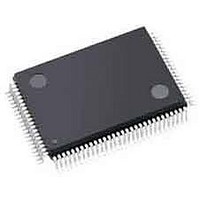
AGLN030V2-ZVQG100 Actel, AGLN030V2-ZVQG100 Datasheet - Page 101

AGLN030V2-ZVQG100
Manufacturer Part Number
AGLN030V2-ZVQG100
Description
FPGA - Field Programmable Gate Array 30K System Gates IGLOO nano
Manufacturer
Actel
Datasheet
1.AGLN030V5-ZUCG81.pdf
(140 pages)
Specifications of AGLN030V2-ZVQG100
Processor Series
AGLN030
Core
IP Core
Number Of Macrocells
256
Maximum Operating Frequency
250 MHz
Number Of Programmable I/os
77
Supply Voltage (max)
1.5 V
Supply Current
6 uA
Maximum Operating Temperature
+ 70 C
Minimum Operating Temperature
- 20 C
Development Tools By Supplier
AGLN-Nano-Kit, AGLN-Z-Nano-Kit, AGL-Dev-Kit-SCS, Silicon-Explorer II, Silicon-Sculptor 3, SI-EX-TCA, FLASHPRO 4, FlashPro 3, FLASHPRO LITE
Mounting Style
SMD/SMT
Supply Voltage (min)
1.2 V
Number Of Gates
30 K
Package / Case
VQFP-100
Lead Free Status / RoHS Status
Lead free / RoHS Compliant
Available stocks
Company
Part Number
Manufacturer
Quantity
Price
Company:
Part Number:
AGLN030V2-ZVQG100
Manufacturer:
Microsemi SoC
Quantity:
10 000
Company:
Part Number:
AGLN030V2-ZVQG100I
Manufacturer:
Microsemi SoC
Quantity:
10 000
JTAG 1532 Characteristics
Table 2-111 • JTAG 1532
Table 2-112 • JTAG 1532
Parameter
t
t
t
t
t
t
F
t
t
t
Note:
Parameter
t
t
t
t
t
t
F
t
t
t
Note:
DISU
DIHD
TMSSU
TMDHD
TCK2Q
RSTB2Q
TRSTREM
TRSTREC
TRSTMPW
DISU
DIHD
TMSSU
TMDHD
TCK2Q
RSTB2Q
TRSTREM
TRSTREC
TRSTMPW
TCKMAX
TCKMAX
For specific junction temperature and voltage supply levels, refer to
For specific junction temperature and voltage supply levels, refer to
JTAG timing delays do not include JTAG I/Os. To obtain complete JTAG timing, add I/O buffer delays to
the corresponding standard selected; refer to the I/O timing characteristics in the
Characteristics" section on page 2-15
Timing Characteristics
1.5 V DC Core Voltage
1.2 V DC Core Voltage
Commercial-Case Conditions: T
Commercial-Case Conditions: T
Test Data Input Setup Time
Test Data Input Hold Time
Test Mode Select Setup Time
Test Mode Select Hold Time
Clock to Q (data out)
Reset to Q (data out)
TCK Maximum Frequency
ResetB Removal Time
ResetB Recovery Time
ResetB Minimum Pulse
Test Data Input Setup Time
Test Data Input Hold Time
Test Mode Select Setup Time
Test Mode Select Hold Time
Clock to Q (data out)
Reset to Q (data out)
TCK Maximum Frequency
ResetB Removal Time
ResetB Recovery Time
ResetB Minimum Pulse
J
J
= 70°C, Worst-Case VCC = 1.425 V
= 70°C, Worst-Case VCC = 1.14 V
for more details.
Description
Description
R ev i si o n 1 1
Table 2-6 on page 2-6
Table 2-6 on page 2-6
IGLOO nano Low Power Flash FPGAs
25.00
TBD
1.00
2.00
1.00
2.00
8.00
0.58
0.00
Std.
11.00
30.00
15
TBD
Std.
1.50
3.00
1.50
3.00
9.00
1.18
0.00
for derating values.
for derating values.
"User I/O
Units
MHz
Units
MHz
ns
ns
ns
ns
ns
ns
ns
ns
ns
ns
ns
ns
ns
ns
ns
ns
ns
ns
2- 87


