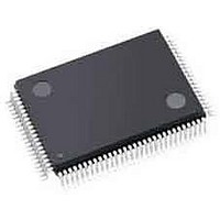
AGLN030V2-ZVQG100 Actel, AGLN030V2-ZVQG100 Datasheet - Page 85

AGLN030V2-ZVQG100
Manufacturer Part Number
AGLN030V2-ZVQG100
Description
FPGA - Field Programmable Gate Array 30K System Gates IGLOO nano
Manufacturer
Actel
Datasheet
1.AGLN030V5-ZUCG81.pdf
(140 pages)
Specifications of AGLN030V2-ZVQG100
Processor Series
AGLN030
Core
IP Core
Number Of Macrocells
256
Maximum Operating Frequency
250 MHz
Number Of Programmable I/os
77
Supply Voltage (max)
1.5 V
Supply Current
6 uA
Maximum Operating Temperature
+ 70 C
Minimum Operating Temperature
- 20 C
Development Tools By Supplier
AGLN-Nano-Kit, AGLN-Z-Nano-Kit, AGL-Dev-Kit-SCS, Silicon-Explorer II, Silicon-Sculptor 3, SI-EX-TCA, FLASHPRO 4, FlashPro 3, FLASHPRO LITE
Mounting Style
SMD/SMT
Supply Voltage (min)
1.2 V
Number Of Gates
30 K
Package / Case
VQFP-100
Lead Free Status / RoHS Status
Lead free / RoHS Compliant
Available stocks
Company
Part Number
Manufacturer
Quantity
Price
Company:
Part Number:
AGLN030V2-ZVQG100
Manufacturer:
Microsemi SoC
Quantity:
10 000
Company:
Part Number:
AGLN030V2-ZVQG100I
Manufacturer:
Microsemi SoC
Quantity:
10 000
Table 2-102 • IGLOO nano CCC/PLL Specification
Parameter
Clock Conditioning Circuitry Input Frequency f
Clock Conditioning Circuitry Output Frequency f
Delay Increments in Programmable Delay Blocks
Number of Programmable Values in Each Programmable Delay Block
Serial Clock (SCLK) for Dynamic PLL
Input Cycle-to-Cycle Jitter (peak magnitude)
Acquisition Time
Tracking Jitter
Output Duty Cycle
Delay Range in Block: Programmable Delay 1
Delay Range in Block: Programmable Delay 2
Delay Range in Block: Fixed Delay
VCO Output Peak-to-Peak Period Jitter F
Notes:
1. This delay is a function of voltage and temperature. See
2. T
3. Maximum value obtained for a STD speed grade device in Worst-Case Commercial conditions. For specific junction
4. Tracking jitter is defined as the variation in clock edge position of PLL outputs with reference to the PLL input clock
5. VCO output jitter is calculated as a percentage of the VCO frequency. The jitter (in ps) can be calculated by multiplying
6. Measurements done with LVTTL 3.3 V 8 mA I/O drive strength and high slew rate. VCC/VCCPLL = 1.14 V,
7. SSOs are outputs that are synchronous to a single clock domain and have their clock-to-out times within ±200 ps of
8. The AGLN010, AGLN015, and AGLN020 devices do not support PLLs.
temperature and voltage supply levels, refer to
edge. Tracking jitter does not measure the variation in PLL output period, which is covered by the period jitter
parameter.
the VCO period by the % jitter. The VCO jitter (in ps) applies to CCC_OUT, regardless of the output divider settings. For
example, if the jitter on VCO is 300 ps, the jitter on CCC_OUT is also 300 ps, no matter what the settings are for the
output divider.
VCCI = 3.3 V, VQ/PQ/TQ type of packages, 20 pF load.
each other. Switching I/Os are placed outside of the PLL bank. Refer to the "ProASIC3/E SSO and Pin Placement
Guidelines" chapter of the
0.75 MHz to 50MHz
50 MHz to 100 MHz
J
= 25°C, V
For IGLOO nano V2 Devices, 1.2 V DC Core Supply Voltage
4
CC
= 1.2 V
ProASIC3 FPGA Fabric User’s
1, 2
3
CCC_OUT
IN_CCC
1, 2
1, 2
OUT_CCC
Table 2-6 on page 2-6
1, 2
5
LockControl = 0
LockControl = 1
LockControl = 0
LockControl = 1
R ev i si o n 1 1
Table 2-6 on page 2-6
Guide.
SSO ≤ 2
0.50
2.50
and
Table 2-7 on page 2-7
SSO ≤ 4
0.025
Min.
0.75
1.20
5.00
48.5
Max Peak-to-Peak Period Jitter
and
2.3
1.5
Table 2-7 on page 2-7
IGLOO nano Low Power Flash FPGAs
SSO ≤ 8 SSO ≤ 16
Typ.
2.00
7.00
580
5.7
for derating values.
20.86
20.86
15.00
Max.
0.25
3.00
160
160
300
51.5
6.0
60
32
4
3
for deratings.
Units
5,6,7
MHz
MHz
ms
ns
ns
ns
%
%
ps
µs
ns
ns
ns
%
2- 71


