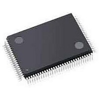
AGLN030V2-ZVQG100 Actel, AGLN030V2-ZVQG100 Datasheet - Page 14

AGLN030V2-ZVQG100
Manufacturer Part Number
AGLN030V2-ZVQG100
Description
FPGA - Field Programmable Gate Array 30K System Gates IGLOO nano
Manufacturer
Actel
Datasheet
1.AGLN030V5-ZUCG81.pdf
(140 pages)
Specifications of AGLN030V2-ZVQG100
Processor Series
AGLN030
Core
IP Core
Number Of Macrocells
256
Maximum Operating Frequency
250 MHz
Number Of Programmable I/os
77
Supply Voltage (max)
1.5 V
Supply Current
6 uA
Maximum Operating Temperature
+ 70 C
Minimum Operating Temperature
- 20 C
Development Tools By Supplier
AGLN-Nano-Kit, AGLN-Z-Nano-Kit, AGL-Dev-Kit-SCS, Silicon-Explorer II, Silicon-Sculptor 3, SI-EX-TCA, FLASHPRO 4, FlashPro 3, FLASHPRO LITE
Mounting Style
SMD/SMT
Supply Voltage (min)
1.2 V
Number Of Gates
30 K
Package / Case
VQFP-100
Lead Free Status / RoHS Status
Lead free / RoHS Compliant
Available stocks
Company
Part Number
Manufacturer
Quantity
Price
Company:
Part Number:
AGLN030V2-ZVQG100
Manufacturer:
Microsemi SoC
Quantity:
10 000
Company:
Part Number:
AGLN030V2-ZVQG100I
Manufacturer:
Microsemi SoC
Quantity:
10 000
IGLOO nano Device Overview
1- 8
For devices using the six CCC block architecture, these are located at the four corners and the centers of
the east and west sides. All six CCC blocks are usable; the four corner CCCs and the east CCC allow
simple clock delay operations as well as clock spine access.
The inputs of the six CCC blocks are accessible from the FPGA core or from dedicated connections to
the CCC block, which are located near the CCC.
The CCC block has these key features:
Additional CCC specifications:
Global Clocking
IGLOO nano devices have extensive support for multiple clocking domains. In addition to the CCC and
PLL support described above, there is a comprehensive global clock distribution network.
Each VersaTile input and output port has access to nine VersaNets: six chip (main) and three quadrant
global networks. The VersaNets can be driven by the CCC or directly accessed from the core via
multiplexers (MUXes). The VersaNets can be used to distribute low-skew clock signals or for rapid
distribution of high-fanout nets.
I/Os with Advanced I/O Standards
IGLOO nano FPGAs feature a flexible I/O structure, supporting a range of voltages (1.2 V, 1.2 V wide
range, 1.5 V, 1.8 V, 2.5 V, 3.0 V wide range, and 3.3 V).
The I/Os are organized into banks with two, three, or four banks per device. The configuration of these
banks determines the I/O standards supported.
Each I/O module contains several input, output, and enable registers. These registers allow the
implementation of various single-data-rate applications for all versions of nano devices and double-data-
rate applications for the AGLN060, AGLN125, and AGLN250 devices.
IGLOO nano devices support LVTTL and LVCMOS I/O standards, are hot-swappable, and support cold-
sparing and Schmitt trigger.
Hot-swap (also called hot-plug, or hot-insertion) is the operation of hot-insertion or hot-removal of a card
in a powered-up system.
Cold-sparing (also called cold-swap) refers to the ability of a device to leave system data undisturbed
when the system is powered up, while the component itself is powered down, or when power supplies
are floating.
Wide Range I/O Support
Actel nano devices support JEDEC-defined wide range I/O operation. IGLOO nano devices support both
the JESD8-B specification, covering both 3 V and 3.3 V supplies, for an effective operating range of
2.7 V to 3.6 V, and JESD8-12 with its 1.2 V nominal, supporting an effective operating range of 1.14 V to
1.575 V.
Wider I/O range means designers can eliminate power supplies or power conditioning components from
the board or move to less costly components with greater tolerances. Wide range eases I/O bank
management and provides enhanced protection from system voltage spikes, while providing the flexibility
to easily run custom voltage applications.
•
•
•
•
•
•
•
•
•
•
Wide input frequency range (f
Output frequency range (f
2 programmable delay types for clock skew minimization
Clock frequency synthesis (for PLL only)
Internal phase shift = 0°, 90°, 180°, and 270°. Output phase shift depends on the output divider
configuration (for PLL only).
Output duty cycle = 50% ± 1.5% or better (for PLL only)
Low output jitter: worst case < 2.5% × clock period peak-to-peak period jitter when single global
network used (for PLL only)
Maximum acquisition time is 300 µs (for PLL only)
Exceptional tolerance to input period jitter—allowable input jitter is up to 1.5 ns (for PLL only)
Four precise phases; maximum misalignment between adjacent phases of 40 ps × 250 MHz /
f
OUT_CCC
(for PLL only)
OUT_CCC
IN_CCC
) = 0.75 MHz up to 250 MHz
) = 1.5 MHz up to 250 MHz
R ev isio n 1 1


