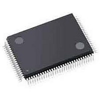
AGLN030V2-ZVQG100 Actel, AGLN030V2-ZVQG100 Datasheet - Page 27

AGLN030V2-ZVQG100
Manufacturer Part Number
AGLN030V2-ZVQG100
Description
FPGA - Field Programmable Gate Array 30K System Gates IGLOO nano
Manufacturer
Actel
Datasheet
1.AGLN030V5-ZUCG81.pdf
(140 pages)
Specifications of AGLN030V2-ZVQG100
Processor Series
AGLN030
Core
IP Core
Number Of Macrocells
256
Maximum Operating Frequency
250 MHz
Number Of Programmable I/os
77
Supply Voltage (max)
1.5 V
Supply Current
6 uA
Maximum Operating Temperature
+ 70 C
Minimum Operating Temperature
- 20 C
Development Tools By Supplier
AGLN-Nano-Kit, AGLN-Z-Nano-Kit, AGL-Dev-Kit-SCS, Silicon-Explorer II, Silicon-Sculptor 3, SI-EX-TCA, FLASHPRO 4, FlashPro 3, FLASHPRO LITE
Mounting Style
SMD/SMT
Supply Voltage (min)
1.2 V
Number Of Gates
30 K
Package / Case
VQFP-100
Lead Free Status / RoHS Status
Lead free / RoHS Compliant
Available stocks
Company
Part Number
Manufacturer
Quantity
Price
Company:
Part Number:
AGLN030V2-ZVQG100
Manufacturer:
Microsemi SoC
Quantity:
10 000
Company:
Part Number:
AGLN030V2-ZVQG100I
Manufacturer:
Microsemi SoC
Quantity:
10 000
1. If a PLL is used to generate more than one output clock, include each output clock in the formula by adding its corresponding
contribution (PAC13* FCLKOUT product) to the total PLL contribution.
Combinatorial Cells Contribution—P
Routing Net Contribution—P
I/O Input Buffer Contribution—P
I/O Output Buffer Contribution—P
RAM Contribution—P
PLL Contribution—P
P
P
P
P
P
P
C-CELL
NET
INPUTS
OUTPUTS
MEMORY
PLL
N
α
page
F
N
N
α
page
F
N
α
F
N
α
β
F
N
F
β
F
β
page
= PDC4 + PAC13 *F
F
= (N
CLK
CLK
CLK
CLK
READ-CLOCK
WRITE-CLOCK
CLKOUT
1
2
3
C-CELL
S-CELL
C-CELL
INPUTS
OUTPUTS
BLOCKS
1
1
2
2
= N
= N
is the I/O buffer enable rate—guidelines are provided in
is the RAM enable rate for read operations.
is the RAM enable rate for write operations—guidelines are provided in
is the I/O buffer toggle rate—guidelines are provided in
is the I/O buffer toggle rate—guidelines are provided in
is the toggle rate of VersaTile outputs—guidelines are provided in
is the toggle rate of VersaTile outputs—guidelines are provided in
S-CELL
= PAC11 * N
= N
is the global clock signal frequency.
is the global clock signal frequency.
is the global clock signal frequency.
is the global clock signal frequency.
2-14.
2-14.
2-14.
C-CELL
INPUTS
OUTPUTS
is the number of VersaTiles used as combinatorial modules in the design.
is the number of VersaTiles used as sequential modules in the design.
is the number of VersaTiles used as combinatorial modules in the design.
is the number of I/O input buffers used in the design.
is the output clock frequency.
is the number of RAM blocks used in the design.
is the number of I/O output buffers used in the design.
+ N
*
*
α
is the memory read clock frequency.
C-CELL
is the memory write clock frequency.
α
PLL
1
MEMORY
BLOCKS
2
/ 2 * PAC7 * F
*
/ 2 * PAC9 * F
α
CLKOUT
) *
2
/ 2 *
α
NET
* F
1
β
/ 2 * PAC8 * F
READ-CLOCK
INPUTS
1
* PAC10 * F
OUTPUTS
CLK
CLK
C-CELL
R ev i si o n 1 1
*
1
CLK
β
CLK
2
+ PAC12 * N
BLOCK
IGLOO nano Low Power Flash FPGAs
Table 2-19 on page
Table 2-19 on page
Table 2-20 on page
* F
WRITE-CLOCK
Table 2-19 on
Table 2-19 on
Table 2-20 on
*
β
2-14.
2-14.
2-14.
3
2- 13


