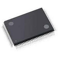
AGLN030V2-ZVQG100 Actel, AGLN030V2-ZVQG100 Datasheet - Page 9

AGLN030V2-ZVQG100
Manufacturer Part Number
AGLN030V2-ZVQG100
Description
FPGA - Field Programmable Gate Array 30K System Gates IGLOO nano
Manufacturer
Actel
Datasheet
1.AGLN030V5-ZUCG81.pdf
(140 pages)
Specifications of AGLN030V2-ZVQG100
Processor Series
AGLN030
Core
IP Core
Number Of Macrocells
256
Maximum Operating Frequency
250 MHz
Number Of Programmable I/os
77
Supply Voltage (max)
1.5 V
Supply Current
6 uA
Maximum Operating Temperature
+ 70 C
Minimum Operating Temperature
- 20 C
Development Tools By Supplier
AGLN-Nano-Kit, AGLN-Z-Nano-Kit, AGL-Dev-Kit-SCS, Silicon-Explorer II, Silicon-Sculptor 3, SI-EX-TCA, FLASHPRO 4, FlashPro 3, FLASHPRO LITE
Mounting Style
SMD/SMT
Supply Voltage (min)
1.2 V
Number Of Gates
30 K
Package / Case
VQFP-100
Lead Free Status / RoHS Status
Lead free / RoHS Compliant
Available stocks
Company
Part Number
Manufacturer
Quantity
Price
Company:
Part Number:
AGLN030V2-ZVQG100
Manufacturer:
Microsemi SoC
Quantity:
10 000
Company:
Part Number:
AGLN030V2-ZVQG100I
Manufacturer:
Microsemi SoC
Quantity:
10 000
† The AGLN030 and smaller devices do not support PLL or SRAM.
valuable intellectual property cannot be compromised or copied. Secure ISP can be performed using the
industry-standard AES algorithm. The IGLOO nano device architecture mitigates the need for ASIC
migration at higher user volumes. This makes IGLOO nano devices cost-effective ASIC replacement
solutions, especially for applications in the consumer, networking/communications, computing, and
avionics markets.
With a variety of devices under $1, Actel IGLOO nano FPGAs enable cost-effective implementation of
programmable logic and quick time to market.
Firm-Error Immunity
Firm errors occur most commonly when high-energy neutrons, generated in the upper atmosphere, strike
a configuration cell of an SRAM FPGA. The energy of the collision can change the state of the
configuration cell and thus change the logic, routing, or I/O behavior in an unpredictable way. These
errors are impossible to prevent in SRAM FPGAs. The consequence of this type of error can be a
complete system failure. Firm errors do not exist in the configuration memory of IGLOO nano flash-based
FPGAs. Once it is programmed, the flash cell configuration element of IGLOO nano FPGAs cannot be
altered by high-energy neutrons and is therefore immune to them. Recoverable (or soft) errors occur in
the user data SRAM of all FPGA devices. These can easily be mitigated by using error detection and
correction (EDAC) circuitry built into the FPGA fabric.
Advanced Flash Technology
The IGLOO nano device offers many benefits, including nonvolatility and reprogrammability, through an
advanced flash-based, 130-nm LVCMOS process with seven layers of metal. Standard CMOS design
techniques are used to implement logic and control functions. The combination of fine granularity,
enhanced flexible routing resources, and abundant flash switches allows for very high logic utilization
without compromising device routability or performance. Logic functions within the device are
interconnected through a four-level routing hierarchy.
IGLOO nano FPGAs utilize design and process techniques to minimize power consumption in all modes
of operation.
Advanced Architecture
The proprietary IGLOO nano architecture provides granularity comparable to standard-cell ASICs. The
IGLOO nano device consists of five distinct and programmable architectural features
page 1-5
The FPGA core consists of a sea of VersaTiles. Each VersaTile can be configured as a three-input logic
function, a D-flip-flop (with or without enable), or a latch by programming the appropriate flash switch
interconnections. The versatility of the IGLOO nano core tile as either a three-input lookup table (LUT)
equivalent or a D-flip-flop/latch with enable allows for efficient use of the FPGA fabric. The VersaTile
capability is unique to the Actel ProASIC
are connected with any of the four levels of routing hierarchy. Flash switches are distributed throughout
the device to provide nonvolatile, reconfigurable interconnect programming. Maximum core utilization is
possible for virtually any design.
In addition, extensive on-chip programming circuitry enables rapid, single-voltage (3.3 V) programming
of IGLOO nano devices via an IEEE 1532 JTAG interface.
•
•
•
•
•
•
Flash*Freeze technology
FPGA VersaTiles
Dedicated FlashROM
Dedicated SRAM/FIFO memory
Extensive CCCs and PLLs
Advanced I/O structure
to
Figure 1-4 on page
1-5):
†
†
®
family of third-generation-architecture flash FPGAs. VersaTiles
R ev i si o n 1 1
IGLOO nano Low Power Flash FPGAs
(Figure 1-3 on
1 -3


