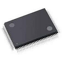
AGLN030V2-ZVQG100 Actel, AGLN030V2-ZVQG100 Datasheet - Page 34

AGLN030V2-ZVQG100
Manufacturer Part Number
AGLN030V2-ZVQG100
Description
FPGA - Field Programmable Gate Array 30K System Gates IGLOO nano
Manufacturer
Actel
Datasheet
1.AGLN030V5-ZUCG81.pdf
(140 pages)
Specifications of AGLN030V2-ZVQG100
Processor Series
AGLN030
Core
IP Core
Number Of Macrocells
256
Maximum Operating Frequency
250 MHz
Number Of Programmable I/os
77
Supply Voltage (max)
1.5 V
Supply Current
6 uA
Maximum Operating Temperature
+ 70 C
Minimum Operating Temperature
- 20 C
Development Tools By Supplier
AGLN-Nano-Kit, AGLN-Z-Nano-Kit, AGL-Dev-Kit-SCS, Silicon-Explorer II, Silicon-Sculptor 3, SI-EX-TCA, FLASHPRO 4, FlashPro 3, FLASHPRO LITE
Mounting Style
SMD/SMT
Supply Voltage (min)
1.2 V
Number Of Gates
30 K
Package / Case
VQFP-100
Lead Free Status / RoHS Status
Lead free / RoHS Compliant
Available stocks
Company
Part Number
Manufacturer
Quantity
Price
Company:
Part Number:
AGLN030V2-ZVQG100
Manufacturer:
Microsemi SoC
Quantity:
10 000
Company:
Part Number:
AGLN030V2-ZVQG100I
Manufacturer:
Microsemi SoC
Quantity:
10 000
- Current page: 34 of 140
- Download datasheet (5Mb)
IGLOO nano DC and Switching Characteristics
Table 2-23 • Summary of AC Measuring Points
Table 2-24 • I/O AC Parameter Definitions
2- 20
Standard
3.3 V LVTTL / 3.3 V LVCMOS
3.3 V LVCMOS Wide Range
2.5 V LVCMOS
1.8 V LVCMOS
1.5 V LVCMOS
1.2 V LVCMOS
1.2 V LVCMOS Wide Range
Parameter
t
t
t
t
t
t
t
t
t
t
t
DP
PY
DOUT
EOUT
DIN
HZ
ZH
LZ
ZL
ZHS
ZLS
Summary of I/O Timing Characteristics – Default I/O Software Settings
Data to Pad delay through the Output Buffer
Pad to Data delay through the Input Buffer
Data to Output Buffer delay through the I/O interface
Enable to Output Buffer Tristate Control delay through the I/O interface
Input Buffer to Data delay through the I/O interface
Enable to Pad delay through the Output Buffer—HIGH to Z
Enable to Pad delay through the Output Buffer—Z to HIGH
Enable to Pad delay through the Output Buffer—LOW to Z
Enable to Pad delay through the Output Buffer—Z to LOW
Enable to Pad delay through the Output Buffer with delayed enable—Z to HIGH
Enable to Pad delay through the Output Buffer with delayed enable—Z to LOW
Parameter Definition
R ev i sio n 1 1
Measuring Trip Point (Vtrip)
0.60 V
0.60 V
0.90 V
0.75 V
1.4 V
1.4 V
1.2 V
Related parts for AGLN030V2-ZVQG100
Image
Part Number
Description
Manufacturer
Datasheet
Request
R

Part Number:
Description:
AGLN030V2-ZCSG81I
Manufacturer:
Actel
Datasheet:

Part Number:
Description:
AGLN030V2-ZQNG48I
Manufacturer:
Actel
Datasheet:

Part Number:
Description:
AGLN030V2-ZQNG68I
Manufacturer:
Actel
Datasheet:

Part Number:
Description:
AGLN030V2-ZUCG81I
Manufacturer:
Actel
Datasheet:

Part Number:
Description:
Manufacturer:
Actel
Datasheet:

Part Number:
Description:
FPGA - Field Programmable Gate Array 30K System Gates IGLOO nano
Manufacturer:
Actel
Datasheet:

Part Number:
Description:
FPGA - Field Programmable Gate Array 30K System Gates IGLOO nano
Manufacturer:
Actel
Datasheet:

Part Number:
Description:
FPGA - Field Programmable Gate Array 30K System Gates IGLOO nano
Manufacturer:
Actel
Datasheet:

Part Number:
Description:
FPGA - Field Programmable Gate Array 30K System Gates IGLOO nano
Manufacturer:
Actel
Datasheet:

Part Number:
Description:
FPGA - Field Programmable Gate Array 30K System Gates IGLOO nano
Manufacturer:
Actel
Datasheet:

Part Number:
Description:
FPGA - Field Programmable Gate Array 30K System Gates IGLOO nano
Manufacturer:
Actel
Datasheet:

Part Number:
Description:
FPGA - Field Programmable Gate Array 30K System Gates IGLOO nano
Manufacturer:
Actel
Datasheet:

Part Number:
Description:
MCU, MPU & DSP Development Tools Silicon Sculptor Programming Mod
Manufacturer:
Actel

Part Number:
Description:
MCU, MPU & DSP Development Tools InSystem Programming ProASICPLUS Devices
Manufacturer:
Actel

Part Number:
Description:
Programming Socket Adapters & Emulators PQ160 Module
Manufacturer:
Actel


