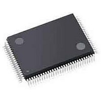
AGLN030V2-ZVQG100 Actel, AGLN030V2-ZVQG100 Datasheet - Page 29

AGLN030V2-ZVQG100
Manufacturer Part Number
AGLN030V2-ZVQG100
Description
FPGA - Field Programmable Gate Array 30K System Gates IGLOO nano
Manufacturer
Actel
Datasheet
1.AGLN030V5-ZUCG81.pdf
(140 pages)
Specifications of AGLN030V2-ZVQG100
Processor Series
AGLN030
Core
IP Core
Number Of Macrocells
256
Maximum Operating Frequency
250 MHz
Number Of Programmable I/os
77
Supply Voltage (max)
1.5 V
Supply Current
6 uA
Maximum Operating Temperature
+ 70 C
Minimum Operating Temperature
- 20 C
Development Tools By Supplier
AGLN-Nano-Kit, AGLN-Z-Nano-Kit, AGL-Dev-Kit-SCS, Silicon-Explorer II, Silicon-Sculptor 3, SI-EX-TCA, FLASHPRO 4, FlashPro 3, FLASHPRO LITE
Mounting Style
SMD/SMT
Supply Voltage (min)
1.2 V
Number Of Gates
30 K
Package / Case
VQFP-100
Lead Free Status / RoHS Status
Lead free / RoHS Compliant
Available stocks
Company
Part Number
Manufacturer
Quantity
Price
Company:
Part Number:
AGLN030V2-ZVQG100
Manufacturer:
Microsemi SoC
Quantity:
10 000
Company:
Part Number:
AGLN030V2-ZVQG100I
Manufacturer:
Microsemi SoC
Quantity:
10 000
User I/O Characteristics
Figure 2-3 • Timing Model
Input LVCMOS 2.5 V
LVCMOS 1.5 V
t
PY
= 0.85 ns
Timing Model
Clock
Input LVTTL
Operating Conditions: STD Speed, Commercial Temperature Range (T
V
CC
= 1.425 V, for DC 1.5 V Core Voltage, Applicable to V2 and V5 Devices
t
PY
(Non-Registered)
(Registered)
= 1.06 ns
t
I/O Module
I/O Module
t
t
PY
ICLKQ
ISUD
= 1.15 ns
= 0.47 ns
= 0.42 ns
D
Q
Register Cell
t
t
CLKQ
SUD
D
= 0.81 ns
= 0.89 ns
Combinational Cell
Q
Combinational Cell
t
PD
Combinational Cell
t
PD
Clock
Input LVTTL
t
PY
= 1.60 ns
t
= 1.18 ns
PD
= 0.85 ns
= 0.91 ns
Combinational Cell
Combinational Cell
Y
Y
t
PD
t
PD
R ev i si o n 1 1
Y
= 1.17 ns
= 0.87 ns
Register Cell
Combinational Cell
t
t
CLKQ
SUD
t
D
PD
Y
Y
= 0.81 ns
(Non-Registered)
= 0.89 ns
= 0.90 ns
I/O Module
t
Q
DP
Clock
t
Input LVTTL
PY
= 2.35 ns
(Non-Registered)
(Non-Registered)
t
t
DP
I/O Module
DP
I/O Module
= 0.85 ns
Y
= 2.65 ns
= 1.96 ns
(Non-Registered)
t
I/O Module
DP
LVTTL Output drive strength = 4 mA
= 1.99 ns
D
t
t
OCLKQ
OSUD
(Registered)
I/O Module
LVTTL Output drive strength = 8 mA
LVCMOS 1.5 V Output drive strength = 2 mA
High slew rate
IGLOO nano Low Power Flash FPGAs
Q
= 0.51 ns
= 1.00 ns
t
DP
High slew rate
= 1.96 ns
LVCMOS 2.5 V Output Drive
Strength = 8 mA High Slew Rate
J
= 70°C), Worst-Case
High slew rate
LVTTL 3.3 V Output drive
strength = 8 mA High slew rate
2- 15


