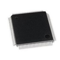
LAN9118-MD SMSC, LAN9118-MD Datasheet - Page 114

LAN9118-MD
Manufacturer Part Number
LAN9118-MD
Description
Ethernet ICs HiPerfrm Sngl-Chip 10/100 Ethrnt
Manufacturer
SMSC
Type
Single Chip MAC and PHYr
Datasheet
1.LAN9118-MT.pdf
(132 pages)
Specifications of LAN9118-MD
Ethernet Connection Type
10 Base-T, 100 Base-TX
Minimum Operating Temperature
0 C
Mounting Style
SMD/SMT
Product
Ethernet Controllers
Number Of Transceivers
1
Standard Supported
802.3
Data Rate
10 MB, 100 MB
Supply Voltage (max)
3.3 V
Supply Voltage (min)
0 V
Maximum Operating Temperature
+ 70 C
Package / Case
TQFP-100
Lead Free Status / RoHS Status
Lead free / RoHS Compliant
- Current page: 114 of 132
- Download datasheet (2Mb)
Chapter 6 Timing Diagrams
Revision 1.5 (07-11-08)
6.1
6.1.1
Read Cycles:
Write Cycles:
The LAN9118 supports the following host cycles:
Special Restrictions on Back-to-Back Write/Read Cycles
It is important to note that there are specific restrictions on the timing of back-to-back write-read
operations. These restrictions concern reading the control registers after any write cycle to the
LAN9118 device. In many cases there is a required minimum delay between writing to the LAN9118,
and the subsequent side effect (change in the control register value). For example, when writing to the
TX Data FIFO, it takes up to 135ns for the level indication to change in the TX_FIFO_INF register.
In order to prevent the host from reading stale data after a write operation, minimum wait periods must
be enforced. These periods are specified in
processor is required to wait the specified period of time after any write to the LAN9118 before reading
the resource specified in the table. These wait periods are for read operations that immediately follow
any write cycle. Note that the required wait period is dependant upon the register being read after the
write.
Performing "dummy" reads of the BYTE_TEST register is a convenient way to guarantee that the
minimum write-to-read timing restriction is met.
are required before reading the register indicated. The number of BYTE_TEST reads in this table is
based on the minimum timing for Tcycle (45ns). For microprocessors with slower busses the number
of reads may be reduced as long as the total time is equal to, or greater than the time specified in the
table. Note that dummy reads of the BYTE_TEST register are not required as long as the minimum
time period is met.
Host Interface Timing
PIO Reads (nCS or nRD controlled)
PIO Burst Reads (nCS or nRD controlled)
RX Data FIFO Direct PIO Reads (nCS or nRD controlled)
RX Data FIFO Direct PIO Burst Reads (nCS or nRD controlled)
PIO writes (nCS and nWR controlled)
TX Data FIFO direct PIO writes (nCS or nWR controlled)
DATASHEET
114
High Performance Single-Chip 10/100 Non-PCI Ethernet Controller
Table 6.1, "Read After Write Timing
Table 6.1
also shows the number of dummy reads that
Rules". The host
SMSC LAN9118
Datasheet
Related parts for LAN9118-MD
Image
Part Number
Description
Manufacturer
Datasheet
Request
R

Part Number:
Description:
IC ETHERNET CTRLR 10/100 100TQFP
Manufacturer:
SMSC
Datasheet:

Part Number:
Description:
MCU, MPU & DSP Development Tools Evaluation Board
Manufacturer:
SMSC

Part Number:
Description:
MCU, MPU & DSP Development Tools Evaluation Board
Manufacturer:
SMSC

Part Number:
Description:
FAST ETHERNET PHYSICAL LAYER DEVICE
Manufacturer:
SMSC Corporation
Datasheet:

Part Number:
Description:
357-036-542-201 CARDEDGE 36POS DL .156 BLK LOPRO
Manufacturer:
SMSC Corporation
Datasheet:

Part Number:
Description:
357-036-542-201 CARDEDGE 36POS DL .156 BLK LOPRO
Manufacturer:
SMSC Corporation
Datasheet:

Part Number:
Description:
357-036-542-201 CARDEDGE 36POS DL .156 BLK LOPRO
Manufacturer:
SMSC Corporation
Datasheet:

Part Number:
Description:
4-PORT USB2.0 HUB CONTROLLER
Manufacturer:
SMSC Corporation
Datasheet:

Part Number:
Description:
Manufacturer:
SMSC Corporation
Datasheet:

Part Number:
Description:
Manufacturer:
SMSC Corporation
Datasheet:

Part Number:
Description:
FDC37C672ENHANCED SUPER I/O CONTROLLER WITH FAST IR
Manufacturer:
SMSC Corporation
Datasheet:

Part Number:
Description:
COM90C66LJPARCNET Controller/Transceiver with AT Interface and On-Chip RAM
Manufacturer:
SMSC Corporation
Datasheet:

Part Number:
Description:
Manufacturer:
SMSC Corporation
Datasheet:

Part Number:
Description:
Manufacturer:
SMSC Corporation
Datasheet:


