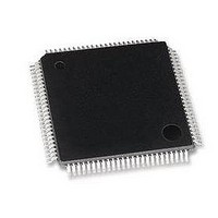
LAN9118-MD SMSC, LAN9118-MD Datasheet - Page 68

LAN9118-MD
Manufacturer Part Number
LAN9118-MD
Description
Ethernet ICs HiPerfrm Sngl-Chip 10/100 Ethrnt
Manufacturer
SMSC
Type
Single Chip MAC and PHYr
Datasheet
1.LAN9118-MT.pdf
(132 pages)
Specifications of LAN9118-MD
Ethernet Connection Type
10 Base-T, 100 Base-TX
Minimum Operating Temperature
0 C
Mounting Style
SMD/SMT
Product
Ethernet Controllers
Number Of Transceivers
1
Standard Supported
802.3
Data Rate
10 MB, 100 MB
Supply Voltage (max)
3.3 V
Supply Voltage (min)
0 V
Maximum Operating Temperature
+ 70 C
Package / Case
TQFP-100
Lead Free Status / RoHS Status
Lead free / RoHS Compliant
- Current page: 68 of 132
- Download datasheet (2Mb)
Revision 1.5 (07-11-08)
5.2.2
5.3
BASE ADDRESS
+ OFFSET
5Ch
6Ch
7Ch
8Ch
50h
54h
58h
60h
64h
68h
70h
74h
78h
80h
84h
88h
90h
94h
98h
TX FIFO Ports
The TX data Path consists of two FIFOs, the TX status and data. The TX Status FIFO can be read
from two locations. The TX Status FIFO Port will perform a destructive read, thus “Popping” the data
from the TX Status FIFO. There is also the TX Status FIFO PEEK location. This location allows a non-
destructive read of the top (oldest) location of the FIFO.
The TX data FIFO is Write Only. It is aliased in 8 DWORD locations (16 WORD locations in 16-bit
mode) from the 20h offset to 3Ch offset. The host may write to any of the 8(16) locations since they
all access the same TX data FIFO location and perform the same function.
Table 5.1, "LAN9118 Direct Address Register
the host bus.
System Control and Status Registers
WORD_SWAP
RX_FIFO_INF
TX_FIFO_INF
BYTE_TEST
RX_DP_CTL
RESERVED
RESERVED
PMT_CTRL
GPIO_CFG
GPT_CFG
GPT_CNT
IRQ_CFG
FIFO_INT
SYMBOL
HW_CFG
INT_STS
RX_CFG
TX_CFG
ID_REV
INT_EN
Table 5.1 LAN9118 Direct Address Register Map
CONTROL AND STATUS REGISTERS
DATASHEET
Chip ID and Revision.
Main Interrupt Configuration
Interrupt Status
Interrupt Enable Register
Reserved for future use
Read-only byte order testing register
FIFO Level Interrupts
Receive Configuration
Transmit Configuration
Hardware Configuration
RX Datapath Control
Receive FIFO Information
Transmit FIFO Information
Power Management Control
General Purpose IO Configuration
General Purpose Timer Configuration
General Purpose Timer Count
Reserved for future use
WORD SWAP Register
68
High Performance Single-Chip 10/100 Non-PCI Ethernet Controller
Map", lists the registers that are directly addressable by
REGISTER NAME
See “ID_REV—
Revision” on
Chip ID and
0000FFFFh
0000FFFFh
00000000h
00000000h
00000000h
87654321h
48000000h
00000000h
00000000h
00050000h
00000000h
00000000h
00001200h
00000000h
00000000h
00000000h
DEFAULT
SMSC LAN9118
page 69.
-
-
Datasheet
Related parts for LAN9118-MD
Image
Part Number
Description
Manufacturer
Datasheet
Request
R

Part Number:
Description:
IC ETHERNET CTRLR 10/100 100TQFP
Manufacturer:
SMSC
Datasheet:

Part Number:
Description:
MCU, MPU & DSP Development Tools Evaluation Board
Manufacturer:
SMSC

Part Number:
Description:
MCU, MPU & DSP Development Tools Evaluation Board
Manufacturer:
SMSC

Part Number:
Description:
FAST ETHERNET PHYSICAL LAYER DEVICE
Manufacturer:
SMSC Corporation
Datasheet:

Part Number:
Description:
357-036-542-201 CARDEDGE 36POS DL .156 BLK LOPRO
Manufacturer:
SMSC Corporation
Datasheet:

Part Number:
Description:
357-036-542-201 CARDEDGE 36POS DL .156 BLK LOPRO
Manufacturer:
SMSC Corporation
Datasheet:

Part Number:
Description:
357-036-542-201 CARDEDGE 36POS DL .156 BLK LOPRO
Manufacturer:
SMSC Corporation
Datasheet:

Part Number:
Description:
4-PORT USB2.0 HUB CONTROLLER
Manufacturer:
SMSC Corporation
Datasheet:

Part Number:
Description:
Manufacturer:
SMSC Corporation
Datasheet:

Part Number:
Description:
Manufacturer:
SMSC Corporation
Datasheet:

Part Number:
Description:
FDC37C672ENHANCED SUPER I/O CONTROLLER WITH FAST IR
Manufacturer:
SMSC Corporation
Datasheet:

Part Number:
Description:
COM90C66LJPARCNET Controller/Transceiver with AT Interface and On-Chip RAM
Manufacturer:
SMSC Corporation
Datasheet:

Part Number:
Description:
Manufacturer:
SMSC Corporation
Datasheet:

Part Number:
Description:
Manufacturer:
SMSC Corporation
Datasheet:


