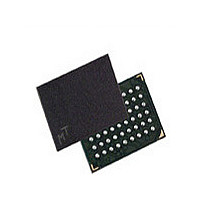
MT48H32M16LFBF-75 IT:B Micron Technology Inc, MT48H32M16LFBF-75 IT:B Datasheet - Page 52

MT48H32M16LFBF-75 IT:B
Manufacturer Part Number
MT48H32M16LFBF-75 IT:B
Description
Manufacturer
Micron Technology Inc
Type
SDRAMr
Datasheet
1.MT48H32M16LFBF-75_ITB.pdf
(86 pages)
Specifications of MT48H32M16LFBF-75 IT:B
Organization
32Mx16
Density
512Mb
Address Bus
15b
Access Time (max)
8/5.4ns
Maximum Clock Rate
133MHz
Operating Supply Voltage (typ)
1.8V
Package Type
VFBGA
Operating Temp Range
-40C to 85C
Operating Supply Voltage (max)
1.95V
Operating Supply Voltage (min)
1.7V
Supply Current
90mA
Pin Count
54
Mounting
Surface Mount
Operating Temperature Classification
Industrial
Lead Free Status / Rohs Status
Compliant
- Current page: 52 of 86
- Download datasheet (3Mb)
Figure 22: Terminating a READ Burst
PDF: 09005aef82ea3742
512mb_mobile_sdram_y47m.pdf – Rev. H 12/09 EN
Note:
Continuous-page READ bursts can be truncated with a BURST TERMINATE command
and fixed-length READ bursts can be truncated with a BURST TERMINATE command,
provided that auto precharge was not activated. The BURST TERMINATE command
should be issued x cycles before the clock edge at which the last desired data element is
valid, where x = CL - 1. This is shown in Figure 22 (page 52) for each possible CAS
latency; data element n + 3 is the last desired data element of a longer burst.
Command
Command
1. DQM is LOW.
Address
Address
CLK
CLK
DQ
DQ
Bank,
T0
Col n
T0
READ
Bank,
READ
Col n
CL = 2
CL = 3
512Mb: 32 Meg x 16, 16 Meg x 32 Mobile SDRAM
T1
T1
NOP
NOP
52
T2
T2
NOP
NOP
D
OUT
Micron Technology, Inc. reserves the right to change products or specifications without notice.
T3
T3
NOP
NOP
D
D
OUT
OUT
TERMINATE
TERMINATE
BURST
BURST
T4
T4
X = 1 cycle
D
D
OUT
OUT
Transitioning data
X = 2 cycles
T5
T5
NOP
NOP
D
D
OUT
OUT
© 2007 Micron Technology, Inc. All rights reserved.
T6
T6
READ Operation
NOP
NOP
D
OUT
Don’t Care
T7
NOP
Related parts for MT48H32M16LFBF-75 IT:B
Image
Part Number
Description
Manufacturer
Datasheet
Request
R

Part Number:
Description:
IC SDRAM 64MBIT 133MHZ 54TSOP
Manufacturer:
Micron Technology Inc
Datasheet:

Part Number:
Description:
IC SDRAM 64MBIT 5.5NS 86TSOP
Manufacturer:
Micron Technology Inc
Datasheet:

Part Number:
Description:
IC SDRAM 64MBIT 200MHZ 86TSOP
Manufacturer:
Micron Technology Inc
Datasheet:

Part Number:
Description:
IC SDRAM 64MBIT 133MHZ 54TSOP
Manufacturer:
Micron Technology Inc
Datasheet:

Part Number:
Description:
IC SDRAM 128MBIT 133MHZ 54TSOP
Manufacturer:
Micron Technology Inc
Datasheet:

Part Number:
Description:
IC SDRAM 256MBIT 133MHZ 90VFBGA
Manufacturer:
Micron Technology Inc
Datasheet:

Part Number:
Description:
IC SDRAM 128MBIT 133MHZ 54TSOP
Manufacturer:
Micron Technology Inc
Datasheet:

Part Number:
Description:
IC SDRAM 256MBIT 133MHZ 54TSOP
Manufacturer:
Micron Technology Inc
Datasheet:

Part Number:
Description:
IC DDR SDRAM 512MBIT 6NS 66TSOP
Manufacturer:
Micron Technology Inc
Datasheet:

Part Number:
Description:
IC SDRAM 128MBIT 167MHZ 86TSOP
Manufacturer:
Micron Technology Inc
Datasheet:

Part Number:
Description:
IC SDRAM 128MBIT 143MHZ 86TSOP
Manufacturer:
Micron Technology Inc
Datasheet:

Part Number:
Description:
SDRAM 256M-BIT 1.8V 54-PIN VFBGA
Manufacturer:
Micron Technology Inc
Datasheet:

Part Number:
Description:
IC SDRAM 128MBIT 143MHZ 86TSOP
Manufacturer:
Micron Technology Inc
Datasheet:

Part Number:
Description:
IC SDRAM 128MBIT 125MHZ 54VFBGA
Manufacturer:
Micron Technology Inc
Datasheet:

Part Number:
Description:
IC SDRAM 128MBIT 125MHZ 54VFBGA
Manufacturer:
Micron Technology Inc
Datasheet:


