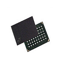
MT48H32M16LFBF-75 IT:B Micron Technology Inc, MT48H32M16LFBF-75 IT:B Datasheet - Page 82

MT48H32M16LFBF-75 IT:B
Manufacturer Part Number
MT48H32M16LFBF-75 IT:B
Description
Manufacturer
Micron Technology Inc
Type
SDRAMr
Datasheet
1.MT48H32M16LFBF-75_ITB.pdf
(86 pages)
Specifications of MT48H32M16LFBF-75 IT:B
Organization
32Mx16
Density
512Mb
Address Bus
15b
Access Time (max)
8/5.4ns
Maximum Clock Rate
133MHz
Operating Supply Voltage (typ)
1.8V
Package Type
VFBGA
Operating Temp Range
-40C to 85C
Operating Supply Voltage (max)
1.95V
Operating Supply Voltage (min)
1.7V
Supply Current
90mA
Pin Count
54
Mounting
Surface Mount
Operating Temperature Classification
Industrial
Lead Free Status / Rohs Status
Compliant
- Current page: 82 of 86
- Download datasheet (3Mb)
Clock Suspend
Figure 50: Clock Suspend During WRITE Burst
PDF: 09005aef82ea3742
512mb_mobile_sdram_y47m.pdf – Rev. H 12/09 EN
Note:
Command
Internal
Address
The clock suspend mode occurs when a column access/burst is in progress and CKE is
registered LOW. In the clock suspend mode, the internal clock is deactivated, freezing
the synchronous logic.
For each positive clock edge on which CKE is sampled LOW, the next internal positive
clock edge is suspended. Any command or data present on the input balls when an in-
ternal clock edge is suspended will be ignored; any data present on the DQ balls
remains driven; and burst counters are not incremented, as long as the clock is suspended.
Exit clock suspend mode by registering CKE HIGH; the internal clock and related opera-
tion will resume on the subsequent positive clock edge.
clock
1. For this example, BL = 4 or greater, and DQM is LOW.
CKE
CLK
D
IN
NOP
T0
WRITE
Bank,
Col n
D
T1
512Mb: 32 Meg x 16, 16 Meg x 32 Mobile SDRAM
IN
T2
82
T3
Micron Technology, Inc. reserves the right to change products or specifications without notice.
NOP
D
T4
IN
Don’t Care
T5
NOP
D
IN
© 2007 Micron Technology, Inc. All rights reserved.
Clock Suspend
Related parts for MT48H32M16LFBF-75 IT:B
Image
Part Number
Description
Manufacturer
Datasheet
Request
R

Part Number:
Description:
IC SDRAM 64MBIT 133MHZ 54TSOP
Manufacturer:
Micron Technology Inc
Datasheet:

Part Number:
Description:
IC SDRAM 64MBIT 5.5NS 86TSOP
Manufacturer:
Micron Technology Inc
Datasheet:

Part Number:
Description:
IC SDRAM 64MBIT 200MHZ 86TSOP
Manufacturer:
Micron Technology Inc
Datasheet:

Part Number:
Description:
IC SDRAM 64MBIT 133MHZ 54TSOP
Manufacturer:
Micron Technology Inc
Datasheet:

Part Number:
Description:
IC SDRAM 128MBIT 133MHZ 54TSOP
Manufacturer:
Micron Technology Inc
Datasheet:

Part Number:
Description:
IC SDRAM 256MBIT 133MHZ 90VFBGA
Manufacturer:
Micron Technology Inc
Datasheet:

Part Number:
Description:
IC SDRAM 128MBIT 133MHZ 54TSOP
Manufacturer:
Micron Technology Inc
Datasheet:

Part Number:
Description:
IC SDRAM 256MBIT 133MHZ 54TSOP
Manufacturer:
Micron Technology Inc
Datasheet:

Part Number:
Description:
IC DDR SDRAM 512MBIT 6NS 66TSOP
Manufacturer:
Micron Technology Inc
Datasheet:

Part Number:
Description:
IC SDRAM 128MBIT 167MHZ 86TSOP
Manufacturer:
Micron Technology Inc
Datasheet:

Part Number:
Description:
IC SDRAM 128MBIT 143MHZ 86TSOP
Manufacturer:
Micron Technology Inc
Datasheet:

Part Number:
Description:
SDRAM 256M-BIT 1.8V 54-PIN VFBGA
Manufacturer:
Micron Technology Inc
Datasheet:

Part Number:
Description:
IC SDRAM 128MBIT 143MHZ 86TSOP
Manufacturer:
Micron Technology Inc
Datasheet:

Part Number:
Description:
IC SDRAM 128MBIT 125MHZ 54VFBGA
Manufacturer:
Micron Technology Inc
Datasheet:

Part Number:
Description:
IC SDRAM 128MBIT 125MHZ 54VFBGA
Manufacturer:
Micron Technology Inc
Datasheet:


