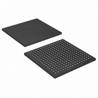
EP3C25U256I7 Altera, EP3C25U256I7 Datasheet - Page 30

EP3C25U256I7
Manufacturer Part Number
EP3C25U256I7
Description
IC CYCLONE III FPGA 25K 256 UBGA
Manufacturer
Altera
Series
Cyclone® IIIr
Datasheets
1.EP3C5F256C8N.pdf
(5 pages)
2.EP3C5F256C8N.pdf
(34 pages)
3.EP3C5F256C8N.pdf
(66 pages)
4.EP3C5F256C8N.pdf
(14 pages)
5.EP3C5F256C8N.pdf
(76 pages)
6.EP3C25U256I7.pdf
(274 pages)
Specifications of EP3C25U256I7
Number Of Logic Elements/cells
24624
Number Of Labs/clbs
1539
Total Ram Bits
608256
Number Of I /o
156
Voltage - Supply
1.15 V ~ 1.25 V
Mounting Type
Surface Mount
Operating Temperature
-40°C ~ 100°C
Package / Case
256-UBGA
Family Name
Cyclone III
Number Of Logic Blocks/elements
24624
# I/os (max)
156
Frequency (max)
437.5MHz
Process Technology
65nm
Operating Supply Voltage (typ)
1.2V
Logic Cells
24624
Ram Bits
608256
Operating Supply Voltage (min)
1.15V
Operating Supply Voltage (max)
1.25V
Operating Temp Range
-40C to 100C
Operating Temperature Classification
Industrial
Mounting
Surface Mount
Pin Count
256
Package Type
UFBGA
For Use With
544-2370 - KIT STARTER CYCLONE III EP3C25
Lead Free Status / RoHS Status
Contains lead / RoHS non-compliant
Number Of Gates
-
Lead Free Status / Rohs Status
Not Compliant
Available stocks
Company
Part Number
Manufacturer
Quantity
Price
Company:
Part Number:
EP3C25U256I7N
Manufacturer:
ALTERA
Quantity:
220
1–20
Table 1–27. Cyclone III Devices Emulated RSDS_E_1R Transmitter Timing Specifications
Table 1–28. Cyclone III Devices Mini-LVDS Transmitter Timing Specifications
Cyclone III Device Handbook, Volume 2
t
t
t
Notes to
(1) Emulated RSDS_E_1R transmitter is supported at the output pin of all I/O banks.
(2) t
f
clock
frequency)
Device
operation in
Mbps
t
TCCS
Output jitter
(peak to
peak)
t
t
t
Notes to
(1) Applicable for true and emulated mini-LVDS transmitter.
(2) True mini-LVDS transmitter is only supported at the output pin of Row I/O (Banks 1, 2, 5, and 6). Emulated mini-LVDS transmitter is supported
(3) t
RISE
FALL
LOCK
HSC LK
DUTY
RISE
FALL
LOCK
Symbol
Symbol
(2)
(3)
at the output pin of all I/O banks.
LOC K
LOC K
(input
Table
Table
is the time required for the PLL to lock from the end of device configuration.
is the time required for the PLL to lock from the end of device configuration.
1–27:
1–28:
20 – 80%,
C
20 – 80%,
C
20 – 80%,
C
20 – 80%,
C
LOAD
LOAD
LOAD
LOAD
Modes
= 5 pF
= 5 pF
Modes
= 5 pF
= 5 pF
—
×10
×10
×8
×7
×4
×2
×1
×8
×7
×4
×2
×1
—
—
—
—
Min
—
—
—
Min
100
10
10
10
10
10
10
80
70
40
20
10
45
—
—
—
—
—
500
500
Typ
C6
—
C6
Typ
500
500
—
—
—
—
—
—
—
—
—
—
—
—
—
—
—
—
Max
Max
200
200
200
200
200
400
400
400
400
400
400
400
200
500
55
—
—
—
—
1
1
Min
100
10
10
10
10
10
10
80
70
40
20
10
45
—
—
—
—
—
Min
—
—
—
C7, I7
C7, I7
500
500
Typ
—
—
—
—
—
—
—
—
—
—
—
—
—
—
—
—
500
500
Typ
—
155.5
155.5
155.5
155.5
155.5
(Note 1)
Max
311
311
311
311
311
311
311
200
500
55
—
—
1
Max
—
—
1
,
(2)
Min
Chapter 1: Cyclone III Device Data Sheet
100
10
10
10
10
10
10
80
70
40
20
10
45
—
—
—
—
—
(Note 1)
Min
—
—
—
© January 2010 Altera Corporation
C8, A7
C8, A7
500
500
Typ
—
—
—
—
—
—
—
—
—
—
—
—
—
—
—
—
500
500
Typ
—
(Part 2 of 2)
Switching Characteristics
155.5
155.5
155.5
155.5
155.5
Max
311
311
311
311
311
311
311
200
550
Max
55
—
—
—
—
1
1
Mbps
Mbps
Mbps
Mbps
Mbps
Mbps
MHz
MHz
MHz
MHz
MHz
MHz
Unit
Unit
ms
ms
ps
ps
ps
ps
ps
ps
%


