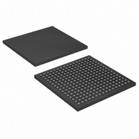
EP3C25U256I7 Altera, EP3C25U256I7 Datasheet - Page 36

EP3C25U256I7
Manufacturer Part Number
EP3C25U256I7
Description
IC CYCLONE III FPGA 25K 256 UBGA
Manufacturer
Altera
Series
Cyclone® IIIr
Datasheets
1.EP3C5F256C8N.pdf
(5 pages)
2.EP3C5F256C8N.pdf
(34 pages)
3.EP3C5F256C8N.pdf
(66 pages)
4.EP3C5F256C8N.pdf
(14 pages)
5.EP3C5F256C8N.pdf
(76 pages)
6.EP3C25U256I7.pdf
(274 pages)
Specifications of EP3C25U256I7
Number Of Logic Elements/cells
24624
Number Of Labs/clbs
1539
Total Ram Bits
608256
Number Of I /o
156
Voltage - Supply
1.15 V ~ 1.25 V
Mounting Type
Surface Mount
Operating Temperature
-40°C ~ 100°C
Package / Case
256-UBGA
Family Name
Cyclone III
Number Of Logic Blocks/elements
24624
# I/os (max)
156
Frequency (max)
437.5MHz
Process Technology
65nm
Operating Supply Voltage (typ)
1.2V
Logic Cells
24624
Ram Bits
608256
Operating Supply Voltage (min)
1.15V
Operating Supply Voltage (max)
1.25V
Operating Temp Range
-40C to 100C
Operating Temperature Classification
Industrial
Mounting
Surface Mount
Pin Count
256
Package Type
UFBGA
For Use With
544-2370 - KIT STARTER CYCLONE III EP3C25
Lead Free Status / RoHS Status
Contains lead / RoHS non-compliant
Number Of Gates
-
Lead Free Status / Rohs Status
Not Compliant
Available stocks
Company
Part Number
Manufacturer
Quantity
Price
Company:
Part Number:
EP3C25U256I7N
Manufacturer:
ALTERA
Quantity:
220
1–26
Table 1–37. Cyclone III Devices IOE Programmable Delay on Column Pins
Table 1–38. Cyclone III Devices IOE Programmable Delay on Row Pins
Cyclone III Device Handbook, Volume 2
Input delay from pin to
internal cells
Input delay from pin to
input register
Delay from output
register to output pin
Input delay from
dual-purpose clock pin
to fan-out destinations
Notes to
(1) The incremental values for the settings are generally linear. For exact values of each setting, use the latest version of the Quartus II software.
(2) The minimum and maximum offset timing numbers are in reference to setting ‘0’ as available in the Quartus II software.
Input delay from pin to
internal cells
Input delay from pin to
input register
Delay from output
register to output pin
Input delay from
dual-purpose clock pin
to fan-out destinations
Notes to
(1) The incremental values for the settings are generally linear. For exact values of each setting, use the latest version of Quartus II software.
(2) The minimum and maximum offset timing numbers are in reference to setting ‘0’ as available in the Quartus II software
Parameter
Parameter
Table
Table
1–37:
1–38:
IOE Programmable Delay
Table 1–37
Pad to I/O
dataout to
core
Pad to I/O
input register
I/O output
register to
pad
Pad to global
clock network
Pad to I/O
dataout to
core
Pad to I/O
input register
I/O output
register to
pad
Pad to global
clock
network
Affected
Affected
Paths
Paths
and
Table 1–38
Settings
Settings
Number
Number
12
12
of
of
7
8
2
7
8
2
Offset
Offset
Min
Min
list IOE programmable delay for Cyclone III devices.
0
0
0
0
0
0
0
0
A7, I7
A7, I7
1.209
1.207
0.669
1.211
1.203
0.479
0.664
0.51
Fast Corner
Fast Corner
1.314
1.312
0.537
0.698
1.314
1.307
0.504
0.694
C6
C6
(Note
(Note
1),
2.174
2.202
0.962
1.207
1),
2.175
0.915
1.199
2.19
C6
C6
(2)
(2)
Max Offset
Max Offset
Chapter 1: Cyclone III Device Data Sheet
2.335
2.402
1.072
1.388
2.387
1.011
1.378
2.32
C7
C7
© January 2010 Altera Corporation
Slow Corner
Slow Corner
2.406
2.558
1.167
1.542
2.386
1.107
1.532
2.54
C8
C8
Switching Characteristics
2.381
2.447
1.074
1.403
2.366
1.018
1.392
2.43
I7
I7
2.505
2.557
1.101
2.545
1.048
1.441
1.45
2.49
A7
A7
Unit
Unit
ns
ns
ns
ns
ns
ns
ns
ns


