EP3C25U256I7 Altera, EP3C25U256I7 Datasheet - Page 35
EP3C25U256I7
Manufacturer Part Number
EP3C25U256I7
Description
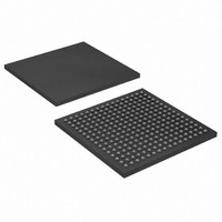
IC CYCLONE III FPGA 25K 256 UBGA
Manufacturer
Altera
Series
Cyclone® IIIr
Datasheets
1.EP3C5F256C8N.pdf
(5 pages)
2.EP3C5F256C8N.pdf
(34 pages)
3.EP3C5F256C8N.pdf
(66 pages)
4.EP3C5F256C8N.pdf
(14 pages)
5.EP3C5F256C8N.pdf
(76 pages)
6.EP3C25U256I7.pdf
(274 pages)
Specifications of EP3C25U256I7
Number Of Logic Elements/cells
24624
Number Of Labs/clbs
1539
Total Ram Bits
608256
Number Of I /o
156
Voltage - Supply
1.15 V ~ 1.25 V
Mounting Type
Surface Mount
Operating Temperature
-40°C ~ 100°C
Package / Case
256-UBGA
Family Name
Cyclone III
Number Of Logic Blocks/elements
24624
# I/os (max)
156
Frequency (max)
437.5MHz
Process Technology
65nm
Operating Supply Voltage (typ)
1.2V
Logic Cells
24624
Ram Bits
608256
Operating Supply Voltage (min)
1.15V
Operating Supply Voltage (max)
1.25V
Operating Temp Range
-40C to 100C
Operating Temperature Classification
Industrial
Mounting
Surface Mount
Pin Count
256
Package Type
UFBGA
For Use With
544-2370 - KIT STARTER CYCLONE III EP3C25
Lead Free Status / RoHS Status
Contains lead / RoHS non-compliant
Number Of Gates
-
Lead Free Status / Rohs Status
Not Compliant
Available stocks
Company
Part Number
Manufacturer
Quantity
Price

Company:
Part Number:
EP3C25U256I7N
Manufacturer:
ALTERA
Quantity:
220


Chapter 1: Cyclone III Device Data Sheet
Switching Characteristics
Table 1–33. Cyclone III Devices Transmitter Channel-to-Channel Skew (TCCS) – Write Side
Table 1–34. Cyclone III Devices Memory Output Clock Jitter Specifications
© January 2010 Altera Corporation
QDRII SRAM
Notes to
(1) Column I/O banks refer to top and bottom I/Os. Row I/O banks refer to right and left I/Os. Wraparound mode refers to the combination of column
(2) For DDR2 SDRAM write timing performance on Columns I/O for C8 and A7 devices, 97.5 degree phase offset is required.
Clock period jitter
Cycle-to-cycle period jitter
Duty cycle jitter
Notes to
(1) The memory output clock jitter measurements are for 200 consecutive clock cycles, as specified in the JEDEC DDR2 standard.
(2) The clock jitter specification applies to memory output clock pins generated using DDIO circuits clocked by a PLL output routed on a global
Standard
Memory
and row I/Os.
clock network.
Table
Table
Parameter
1–33:
1–34:
1.8 V HSTL Class I
1.8 V HSTL Class II
Table 1–34
Duty Cycle Distortion Specifications
Table 1–35
Table 1–35. Duty Cycle Distortion on Cyclone III Devices I/O Pins
OCT Calibration Timing Specification
Table 1–36
power-up for Cyclone III devices.
Table 1–36. Cyclone III Devices Timing Specification for Series OCT with Calibration at Device
Power-Up
I/O Standard
Output Duty Cycle
Notes to
(1) Duty cycle distortion specification applies to clock outputs from PLLs, global clock tree, and IOE driving dedicated
(2) Cyclone III devices meet specified duty cycle distortion at maximum output toggle rate for each combination of
t
Notes to
(1) OCT calibration takes place after device configuration, before entering user mode.
OCTC AL
and general purpose I/O pins.
I/O standard and current strength.
Table
Table
Symbol
Symbol
(Note 1)
lists the memory output clock jitter specifications for Cyclone III devices.
lists the worst case duty cycle distortion for Cyclone III devices.
lists the duration of calibration for series OCT with calibration at device
1–35:
1–36:
Symbol
t
t
t
JIT(duty)
JIT(per)
JIT(cc)
Lead
1092
1250
Column I/Os (ps)
Duration of series OCT with
calibration at device power-up
Min
45
515
662
Lag
C6
Max
55
Description
-125
-200
-150
Min
Lead
1092
1250
(Note
Min
Row I/Os (ps)
45
C7, I7
1),
(2)
Max
55
Lag
515
662
Max
125
200
150
Cyclone III Device Handbook, Volume 2
(Note 1)
(Note
Min
45
Maximum
Wraparound Mode (ps)
C8, A7
1),
1192
1350
Lead
20
(Part 2 of 2)
(2)
Max
55
Unit
ps
ps
ps
615
762
Lag
Unit
Unit
%
µs
1–25
Related parts for EP3C25U256I7
Image
Part Number
Description
Manufacturer
Datasheet
Request
R

Part Number:
Description:
CYCLONE II STARTER KIT EP2C20N
Manufacturer:
Altera
Datasheet:


Part Number:
Description:
CPLD, EP610 Family, ECMOS Process, 300 Gates, 16 Macro Cells, 16 Reg., 16 User I/Os, 5V Supply, 35 Speed Grade, 24DIP
Manufacturer:
Altera Corporation
Datasheet:
Part Number:
Description:
CPLD, EP610 Family, ECMOS Process, 300 Gates, 16 Macro Cells, 16 Reg., 16 User I/Os, 5V Supply, 15 Speed Grade, 24DIP
Manufacturer:
Altera Corporation
Datasheet:
Part Number:
Description:
Manufacturer:
Altera Corporation
Datasheet:
Part Number:
Description:
CPLD, EP610 Family, ECMOS Process, 300 Gates, 16 Macro Cells, 16 Reg., 16 User I/Os, 5V Supply, 30 Speed Grade, 24DIP
Manufacturer:
Altera Corporation
Datasheet:
Part Number:
Description:
High-performance, low-power erasable programmable logic devices with 8 macrocells, 10ns
Manufacturer:
Altera Corporation
Datasheet:
Part Number:
Description:
High-performance, low-power erasable programmable logic devices with 8 macrocells, 7ns
Manufacturer:
Altera Corporation
Datasheet:
Part Number:
Description:
Classic EPLD
Manufacturer:
Altera Corporation
Datasheet:
Part Number:
Description:
High-performance, low-power erasable programmable logic devices with 8 macrocells, 10ns
Manufacturer:
Altera Corporation
Datasheet:
Part Number:
Description:
Manufacturer:
Altera Corporation
Datasheet:
Part Number:
Description:
Manufacturer:
Altera Corporation
Datasheet:
Part Number:
Description:
Manufacturer:
Altera Corporation
Datasheet:
Part Number:
Description:
CPLD, EP610 Family, ECMOS Process, 300 Gates, 16 Macro Cells, 16 Reg., 16 User I/Os, 5V Supply, 25 Speed Grade, 24DIP
Manufacturer:
Altera Corporation
Datasheet: