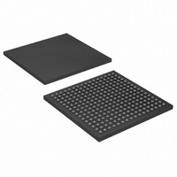
EP3C25U256I7 Altera, EP3C25U256I7 Datasheet - Page 74

EP3C25U256I7
Manufacturer Part Number
EP3C25U256I7
Description
IC CYCLONE III FPGA 25K 256 UBGA
Manufacturer
Altera
Series
Cyclone® IIIr
Datasheets
1.EP3C5F256C8N.pdf
(5 pages)
2.EP3C5F256C8N.pdf
(34 pages)
3.EP3C5F256C8N.pdf
(66 pages)
4.EP3C5F256C8N.pdf
(14 pages)
5.EP3C5F256C8N.pdf
(76 pages)
6.EP3C25U256I7.pdf
(274 pages)
Specifications of EP3C25U256I7
Number Of Logic Elements/cells
24624
Number Of Labs/clbs
1539
Total Ram Bits
608256
Number Of I /o
156
Voltage - Supply
1.15 V ~ 1.25 V
Mounting Type
Surface Mount
Operating Temperature
-40°C ~ 100°C
Package / Case
256-UBGA
Family Name
Cyclone III
Number Of Logic Blocks/elements
24624
# I/os (max)
156
Frequency (max)
437.5MHz
Process Technology
65nm
Operating Supply Voltage (typ)
1.2V
Logic Cells
24624
Ram Bits
608256
Operating Supply Voltage (min)
1.15V
Operating Supply Voltage (max)
1.25V
Operating Temp Range
-40C to 100C
Operating Temperature Classification
Industrial
Mounting
Surface Mount
Pin Count
256
Package Type
UFBGA
For Use With
544-2370 - KIT STARTER CYCLONE III EP3C25
Lead Free Status / RoHS Status
Contains lead / RoHS non-compliant
Number Of Gates
-
Lead Free Status / Rohs Status
Not Compliant
Available stocks
Company
Part Number
Manufacturer
Quantity
Price
Company:
Part Number:
EP3C25U256I7N
Manufacturer:
ALTERA
Quantity:
220
2–30
Table 2–39. Glossary (Part 5 of 5)
Cyclone III Device Handbook, Volume 2
Letter
W
V
X
Y
Z
V
V
V
V
V
V
V
V
V
V
V
V
V
V
V
V
V
V
V
V
V
V
V
V
V
C M( DC)
DIF( AC )
DIF( DC)
IC M
ID
IH
IH(A C)
IH(DC )
IL
IL ( AC )
IL ( DC)
IN
OC M
OD
OH
OL
OS
OX ( AC)
REF
REF (A C)
REF (DC )
S WING (A C)
S WING (DC )
TT
X ( AC)
Term
—
—
—
—
DC common mode input voltage.
AC differential Input Voltage—The minimum AC input differential voltage required for
switching.
DC differential Input Voltage—The minimum DC input differential voltage required for
switching.
Input Common Mode Voltage—The common mode of the differential signal at the receiver.
Input differential Voltage Swing—The difference in voltage between the positive and
complementary conductors of a differential transmission at the receiver.
Voltage Input High—The minimum positive voltage applied to the input that is accepted by
the device as a logic high.
High-level AC input voltage.
High-level DC input voltage.
Voltage Input Low—The maximum positive voltage applied to the input that is accepted by
the device as a logic low.
Low-level AC input voltage.
Low-level DC input voltage.
DC input voltage.
Output Common Mode Voltage—The common mode of the differential signal at the
transmitter.
Output differential Voltage Swing—The difference in voltage between the positive and
complementary conductors of a differential transmission at the transmitter. V
Voltage Output High—The maximum positive voltage from an output that the device
considers will be accepted as the minimum positive high level.
Voltage Output Low—The maximum positive voltage from an output that the device considers
will be accepted as the maximum positive low level.
Output offset voltage—V
AC differential Output cross point voltage—The voltage at which the differential output signals
must cross.
Reference voltage for the SSTL and HSTL I/O standards.
AC input reference voltage for the SSTL and HSTL I/O standards. V
peak-to-peak AC noise on V
DC input reference voltage for the SSTL and HSTL I/O standards.
AC differential Input Voltage—AC Input differential voltage required for switching. Refer to
Input Waveforms for the SSTL Differential I/O Standard.
DC differential Input Voltage—DC Input differential voltage required for switching. Refer to
Input Waveforms for the SSTL Differential I/O Standard.
Termination voltage for the SSTL and HSTL I/O standards.
AC differential Input cross point Voltage—The voltage at which the differential input signals
must cross.
OS
= (V
REF
must not exceed 2% of V
OH
+ V
OL
) / 2.
Definitions
—
—
—
—
REF (DC)
Chapter 2: Cyclone III LS Device Data Sheet
.
© December 2009 Altera Corporation
REF (AC )
= V
REF (DC)
OD
= V
+ noise. The
OH
– V
Glossary
OL
.


