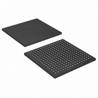
EP3C25U256I7 Altera, EP3C25U256I7 Datasheet - Page 66

EP3C25U256I7
Manufacturer Part Number
EP3C25U256I7
Description
IC CYCLONE III FPGA 25K 256 UBGA
Manufacturer
Altera
Series
Cyclone® IIIr
Datasheets
1.EP3C5F256C8N.pdf
(5 pages)
2.EP3C5F256C8N.pdf
(34 pages)
3.EP3C5F256C8N.pdf
(66 pages)
4.EP3C5F256C8N.pdf
(14 pages)
5.EP3C5F256C8N.pdf
(76 pages)
6.EP3C25U256I7.pdf
(274 pages)
Specifications of EP3C25U256I7
Number Of Logic Elements/cells
24624
Number Of Labs/clbs
1539
Total Ram Bits
608256
Number Of I /o
156
Voltage - Supply
1.15 V ~ 1.25 V
Mounting Type
Surface Mount
Operating Temperature
-40°C ~ 100°C
Package / Case
256-UBGA
Family Name
Cyclone III
Number Of Logic Blocks/elements
24624
# I/os (max)
156
Frequency (max)
437.5MHz
Process Technology
65nm
Operating Supply Voltage (typ)
1.2V
Logic Cells
24624
Ram Bits
608256
Operating Supply Voltage (min)
1.15V
Operating Supply Voltage (max)
1.25V
Operating Temp Range
-40C to 100C
Operating Temperature Classification
Industrial
Mounting
Surface Mount
Pin Count
256
Package Type
UFBGA
For Use With
544-2370 - KIT STARTER CYCLONE III EP3C25
Lead Free Status / RoHS Status
Contains lead / RoHS non-compliant
Number Of Gates
-
Lead Free Status / Rohs Status
Not Compliant
Available stocks
Company
Part Number
Manufacturer
Quantity
Price
Company:
Part Number:
EP3C25U256I7N
Manufacturer:
ALTERA
Quantity:
220
2–22
Table 2–32. FPGA Sampling Window (SW) Requirement—Read Side
Cyclone III Device Handbook, Volume 2
DDR2 SDRAM
DDR SDRAM
QDRII SRAM
DDR2 SDRAM
DDR SDRAM
QDRII SRAM
DDR2 SDRAM
DDR SDRAM
QDRII SRAM
Note to
(1) Column I/Os refer to top and bottom I/Os. Row I/Os refer to right and left I/Os. Wraparound mode refers to the combination of column and row
I/Os.
Memory Standard
Table
2–32:
f
Table 2–31. Cyclone III LS Devices LVDS Receiver Timing Specifications
External Memory Interface Specifications
Cyclone III LS devices support external memory interfaces up to 200 MHz. The
external memory interfaces for Cyclone III LS devices are auto-calibrating and easy to
implement.
Table 2–32
Cyclone III LS devices and are useful when performing memory interface timing
analysis.
For more information about external memory system specifications, refer to the
External Memory Interface
(Part 2 of 2) (Preliminary)
Input jitter
tolerance
t
Notes to
(1) True LVDS receiver is supported at all banks.
(2) t
LOCK
(2)
LOC K
Symbol
Table
is the time required for the PLL to lock from the end of device configuration.
and
Setup
1050
705
675
900
785
800
765
745
945
2–31:
Column I/Os (ps)
Table 2–33
Modes
—
—
Hold
650
620
845
720
740
990
710
690
890
Handbook.
list the external memory interface specifications for
C7
C8
I7
Min
—
—
Setup
1065
C7 and I7
770
795
910
930
915
855
880
955
(Note 1)
Row I/Os (ps)
Max
500
1
(Preliminary)
Hold
1005
715
740
855
870
855
800
825
900
Chapter 2: Cyclone III LS Device Data Sheet
© December 2009 Altera Corporation
Min
—
—
Wraparound Mode (ps)
(Note 1)
Setup
1185
1210
1040
1000
1085
1115
1130
C8
985
970
Switching Characteristics
Max
550
1
1030
1055
1125
1150
1075
Hold
930
915
985
945
Unit
ps
ps


