EP3C25U256I7 Altera, EP3C25U256I7 Datasheet - Page 40
EP3C25U256I7
Manufacturer Part Number
EP3C25U256I7
Description
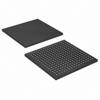
IC CYCLONE III FPGA 25K 256 UBGA
Manufacturer
Altera
Series
Cyclone® IIIr
Datasheets
1.EP3C5F256C8N.pdf
(5 pages)
2.EP3C5F256C8N.pdf
(34 pages)
3.EP3C5F256C8N.pdf
(66 pages)
4.EP3C5F256C8N.pdf
(14 pages)
5.EP3C5F256C8N.pdf
(76 pages)
6.EP3C25U256I7.pdf
(274 pages)
Specifications of EP3C25U256I7
Number Of Logic Elements/cells
24624
Number Of Labs/clbs
1539
Total Ram Bits
608256
Number Of I /o
156
Voltage - Supply
1.15 V ~ 1.25 V
Mounting Type
Surface Mount
Operating Temperature
-40°C ~ 100°C
Package / Case
256-UBGA
Family Name
Cyclone III
Number Of Logic Blocks/elements
24624
# I/os (max)
156
Frequency (max)
437.5MHz
Process Technology
65nm
Operating Supply Voltage (typ)
1.2V
Logic Cells
24624
Ram Bits
608256
Operating Supply Voltage (min)
1.15V
Operating Supply Voltage (max)
1.25V
Operating Temp Range
-40C to 100C
Operating Temperature Classification
Industrial
Mounting
Surface Mount
Pin Count
256
Package Type
UFBGA
For Use With
544-2370 - KIT STARTER CYCLONE III EP3C25
Lead Free Status / RoHS Status
Contains lead / RoHS non-compliant
Number Of Gates
-
Lead Free Status / Rohs Status
Not Compliant
Available stocks
Company
Part Number
Manufacturer
Quantity
Price

Company:
Part Number:
EP3C25U256I7N
Manufacturer:
ALTERA
Quantity:
220


1–30
Table 1–39. Glossary (Part 4 of 5)
Cyclone III Device Handbook, Volume 2
Letter
U
T
t
TCCS (Channel-
to-channel-skew)
tcin
t
tcout
t
t
t
Timing Unit
Interval (TUI)
t
t
t
tpllcin
tpllcout
Transmitter
Output Waveform
t
t
C
C O
DUTY
FA LL
H
INJITTER
OUTJITTER_DEDC LK
OUTJITTER_IO
RISE
S U
Term
—
High-speed receiver/transmitter input and output clock period.
HIGH-SPEED I/O Block: The timing difference between the fastest and slowest output edges,
including t
Delay from clock pad to I/O input register.
Delay from clock pad to I/O output.
Delay from clock pad to I/O output register.
HIGH-SPEED I/O Block: Duty cycle on high-speed transmitter output clock.
Signal High-to-low transition time (80–20%).
Input register hold time.
HIGH-SPEED I/O block: The timing budget allowed for skew, propagation delays, and data
sampling window. (TUI = 1/(Receiver Input Clock Frequency Multiplication Factor) = t
Period jitter on PLL clock input.
Period jitter on dedicated clock output driven by a PLL.
Period jitter on general purpose I/O driven by a PLL.
Delay from PLL inclk pad to I/O input register.
Delay from PLL inclk pad to I/O output register.
Transmitter Output Waveforms for the LVDS, mini-LVDS, PPDS and RSDS Differential I/O
Standards
Signal Low-to-high transition time (20–80%).
Input register setup time.
Single-Ended Waveform
Differential Waveform (Mathematical Function of Positive & Negative Channel)
C O
variation and clock skew. The clock is included in the TCCS measurement.
V os
V
OD
V
OD
Definitions
—
Chapter 1: Cyclone III Device Data Sheet
V
OD
© January 2010 Altera Corporation
Positive Channel (p) = V
Negative Channel (n) = V
Ground
0 V
p - n
C
/w).
OH
OL
Glossary
Related parts for EP3C25U256I7
Image
Part Number
Description
Manufacturer
Datasheet
Request
R

Part Number:
Description:
CYCLONE II STARTER KIT EP2C20N
Manufacturer:
Altera
Datasheet:


Part Number:
Description:
CPLD, EP610 Family, ECMOS Process, 300 Gates, 16 Macro Cells, 16 Reg., 16 User I/Os, 5V Supply, 35 Speed Grade, 24DIP
Manufacturer:
Altera Corporation
Datasheet:
Part Number:
Description:
CPLD, EP610 Family, ECMOS Process, 300 Gates, 16 Macro Cells, 16 Reg., 16 User I/Os, 5V Supply, 15 Speed Grade, 24DIP
Manufacturer:
Altera Corporation
Datasheet:
Part Number:
Description:
Manufacturer:
Altera Corporation
Datasheet:
Part Number:
Description:
CPLD, EP610 Family, ECMOS Process, 300 Gates, 16 Macro Cells, 16 Reg., 16 User I/Os, 5V Supply, 30 Speed Grade, 24DIP
Manufacturer:
Altera Corporation
Datasheet:
Part Number:
Description:
High-performance, low-power erasable programmable logic devices with 8 macrocells, 10ns
Manufacturer:
Altera Corporation
Datasheet:
Part Number:
Description:
High-performance, low-power erasable programmable logic devices with 8 macrocells, 7ns
Manufacturer:
Altera Corporation
Datasheet:
Part Number:
Description:
Classic EPLD
Manufacturer:
Altera Corporation
Datasheet:
Part Number:
Description:
High-performance, low-power erasable programmable logic devices with 8 macrocells, 10ns
Manufacturer:
Altera Corporation
Datasheet:
Part Number:
Description:
Manufacturer:
Altera Corporation
Datasheet:
Part Number:
Description:
Manufacturer:
Altera Corporation
Datasheet:
Part Number:
Description:
Manufacturer:
Altera Corporation
Datasheet:
Part Number:
Description:
CPLD, EP610 Family, ECMOS Process, 300 Gates, 16 Macro Cells, 16 Reg., 16 User I/Os, 5V Supply, 25 Speed Grade, 24DIP
Manufacturer:
Altera Corporation
Datasheet: