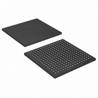
EP3C25U256I7 Altera, EP3C25U256I7 Datasheet - Page 53

EP3C25U256I7
Manufacturer Part Number
EP3C25U256I7
Description
IC CYCLONE III FPGA 25K 256 UBGA
Manufacturer
Altera
Series
Cyclone® IIIr
Datasheets
1.EP3C5F256C8N.pdf
(5 pages)
2.EP3C5F256C8N.pdf
(34 pages)
3.EP3C5F256C8N.pdf
(66 pages)
4.EP3C5F256C8N.pdf
(14 pages)
5.EP3C5F256C8N.pdf
(76 pages)
6.EP3C25U256I7.pdf
(274 pages)
Specifications of EP3C25U256I7
Number Of Logic Elements/cells
24624
Number Of Labs/clbs
1539
Total Ram Bits
608256
Number Of I /o
156
Voltage - Supply
1.15 V ~ 1.25 V
Mounting Type
Surface Mount
Operating Temperature
-40°C ~ 100°C
Package / Case
256-UBGA
Family Name
Cyclone III
Number Of Logic Blocks/elements
24624
# I/os (max)
156
Frequency (max)
437.5MHz
Process Technology
65nm
Operating Supply Voltage (typ)
1.2V
Logic Cells
24624
Ram Bits
608256
Operating Supply Voltage (min)
1.15V
Operating Supply Voltage (max)
1.25V
Operating Temp Range
-40C to 100C
Operating Temperature Classification
Industrial
Mounting
Surface Mount
Pin Count
256
Package Type
UFBGA
For Use With
544-2370 - KIT STARTER CYCLONE III EP3C25
Lead Free Status / RoHS Status
Contains lead / RoHS non-compliant
Number Of Gates
-
Lead Free Status / Rohs Status
Not Compliant
Available stocks
Company
Part Number
Manufacturer
Quantity
Price
Company:
Part Number:
EP3C25U256I7N
Manufacturer:
ALTERA
Quantity:
220
Chapter 2: Cyclone III LS Device Data Sheet
Electrical Characteristics
Table 2–10. Cyclone III LS Devices Internal Weak Pull-Up Weak and Pull-Down Resistor
© December 2009
R
R
Notes to
(1) All I/O pins have an option to enable weak pull-up except the configuration, test, and JTAG pins. The weak pull-down feature is only available
(2) Pin pull-up resistance values may be lower if an external source drives the pin higher than V
(3) R
(4) R
_P U
_P D
Symbol
for JTAG TCK.
Minimum condition: –40°C; V
Typical condition: 25°C; V
Maximum condition: 125°C; V
Minimum condition: –40°C; V
Typical condition: 25°C; V
Maximum condition: 125°C; V
_P U
_P D
Table
= (V
= V
I
/I
CCIO
R_PD
Value of I/O pin pull-up resistor before
and during configuration, as well as
user mode if the programmable
pull-up resistor option is enabled
Value of I/O pin pull-down resistor
before and during configuration
2–10:
– V
Altera Corporation
I
)/I
R_PU
Internal Weak Pull-Up and Weak Pull-Down Resistor
Table 2–10
devices.
Hot Socketing
Table 2–11
Table 2–11. Cyclone III Devices LS Hot-Socketing Specifications
I
I
Note to
(1) The I/O ramp rate is 10 ns or more. For ramp rates faster than 10 ns, |IIOPIN| = C dv/dt, in which C is I/O pin
IOPIN(DC )
IOPIN(A C)
CC IO
CC IO
Parameter
capacitance and dv/dt is the slew rate.
CC IO
= V
CC IO
= V
CCIO
CCIO
Table
C C
C C
= V
= V
= V
= V
, V
, V
Symbol
C C
C C
I
CC
I
CC
lists the hot-socketing specifications for Cyclone III LS devices.
lists the weak pull-up and pull-down resistor values for Cyclone III LS
= 0 V;
= V
2–11:
+ 5%, V
+ 5%, V
– 5% , V
– 5% , V
CC
– 5% ;
I
I
I
I
= V
= 50 mV;
= 0 V; in which V
= V
CC
C C
+ 5% – 50 mV;
– 5% ; in which V
V
V
V
V
V
V
V
V
V
V
V
DC current per I/O pin
AC current per I/O pin
CC IO
CC IO
CC IO
CC IO
CC IO
CC IO
CC IO
CC IO
CC IO
CC IO
CC IO
= 3.3 V ± 5% (2),
= 3.0 V ± 5% (2),
= 2.5 V ± 5% (2),
= 1.8 V ± 5% (2),
= 1.5 V ± 5% (2),
= 1.2 V ± 5% (2),
= 3.3 V ± 5%
= 3.0 V ± 5%
= 2.5 V ± 5%
= 1.8 V ± 5%
= 1.5 V ± 5%
I
refers to the input voltage at the I/O pin.
Parameter
I
Conditions
refers to the input voltage at the I/O pin.
(4)
(4)
(4)
(4)
(4)
(3)
(3)
(3)
(3)
(3)
(3)
CCIO
.
(Note 1)
Cyclone III Device Handbook, Volume 2
Min
10
13
19
7
7
8
6
6
6
7
8
Maximum
8 mA
Typ
143
300 μA
25
28
35
57
82
19
22
25
35
50
(1)
Max
108
163
351
112
41
47
61
30
36
43
71
Unit
kΩ
kΩ
kΩ
kΩ
kΩ
kΩ
kΩ
kΩ
kΩ
kΩ
kΩ
2–9


