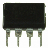
FMS7401LEN Fairchild Semiconductor, FMS7401LEN Datasheet - Page 14

FMS7401LEN
Manufacturer Part Number
FMS7401LEN
Description
IC CTRLR POWER DGTL EEPROM 8DIP
Manufacturer
Fairchild Semiconductor
Datasheet
1.FMS7401LVN.pdf
(81 pages)
Specifications of FMS7401LEN
Applications
Digital Power Controller
Core Processor
8-Bit
Program Memory Type
EEPROM (1 kB)
Ram Size
64 x 8
Number Of I /o
6
Voltage - Supply
2.7 V ~ 3.6 V
Operating Temperature
-40°C ~ 85°C
Mounting Type
Through Hole
Package / Case
8-DIP (0.300", 7.62mm)
Mounting Style
Through Hole
Lead Free Status / RoHS Status
Lead free / RoHS Compliant
Interface
-
Controller Series
-
Lead Free Status / Rohs Status
Lead free / RoHS Compliant
Other names
FMS7401LEN_NL
FMS7401LEN_NL
FMS7401LEN_NL
Available stocks
Company
Part Number
Manufacturer
Quantity
Price
Company:
Part Number:
FMS7401LEN14
Manufacturer:
Rohm
Quantity:
21 626
FMS7401L
enabled, it must complete the lock phase before software may enable the use of the outputs to clock any of the device circuits.
Therefore, upon exiting Halt Mode software must wait the T
frequency and in phase.
1.
2.
3. Prior to entering Halt Mode, software must clear both FMODE and FSEL (the PWM Timer 1 must be disabled in order to
4. Using a separate instruction (e.g. RBIT PLLEN, PSCALE) disable the PLL by clearing the PLLEN bit.
5. Software may then instruct the device to enter Halt Mode.
6. If all disabled circuits must be re-enabled after exiting from Halt Mode, repeat all initial steps enabling all
3.2
In addition to the Halt Mode power saving feature, the device also supports an Idle Mode operation. The device is placed into
Idle Mode by setting the Idle enable bit (EIDLE) of the HALT register through software using either the “LD M, #” or the
“SBIT #, M” instructions. EIDLE is a write only bit and is automatically cleared upon exiting Idle Mode. The Idle Mode
operation is similar to Halt Mode except the internal oscillator, PLL, and Timer 0 circuits remain active while the other on-chip
systems including the Programmable Comparator (COMP) and Brown-out Reset (BOR) circuits are shut down.
The device exits Idle Mode automatically by the Timer 0 Idle overflow every 8192 cycles and by the Multi-input Wakeup
(MIW) circuit.
out waiting for the overflow to occur. Once a wake from Idle Mode is triggered, the normal device execution resumes by the
next clock cycle. Immediately after exiting Idle Mode, software must clear the Power Mode Clear (PMC) register by using only
the “LD M, #” instruction (see
3.2.1 PLL Steps for Idle Mode
When using Idle Mode, the PLL does not need to be disabled prior to entering Idle as it does with Halt Mode. The PLL may
remain enabled the entire time the device is in Idle; however, the device will consume additional current. If current consump-
tion is important, consider using Halt instead of Idle Mode or at least disabling the PLL while in Idle.
By keeping the PLL enabled while in Idle Mode, the PLL’s outputs remain ready for use at any moment. With the PLL’s out-
puts available, software has the option to source the main system clock (F
bit of the PSCALE register is set.
may remain operational while in Idle Mode. However, the total current consumption will increase, hence the recommendation
to disable the PWM Timer 1 before entering Idle Mode. In contrast, if F
execution (like the main system controller) is stopped during Idle. Whether the PWM Timer 1 is operational or not during Idle
Mode, the instruction execution is stopped therefore all pending flags, etc. cannot be serviced.
If the PLL is to be disabled prior to entering Idle Mode, software must take the appropriate steps in order to keep the integrity
of the clock structure. Once the PLL is disabled, all output frequencies are turned off. If the PLL is re-enabled, it must com-
plete the lock phase before software may enable the use of the outputs to clock any of the device circuits. Therefore, upon exit-
ing Idle Mode software must wait the T
14
Initially, the PLLEN bit of the PSCALE register must be set in order to enable the PLL circuit.
If the PLL outputs are to be used to clock any of the device circuits, FMODE and/or FSEL of the PSCALE register must
be set after the appropriate T
clear either bit) keeping the PLLEN bit 1.
circuits in the appropriate order as well as waiting T
Idle Mode
1
Software must first configure the MIW prior to entering Idle Mode in order to wake the device from Idle with-
Figure
PLL_LOCK
3
In addition, if the PLL’s F
5).
PLL_LOCK
wait time.
to ensure that the PLL is locked into its appropriate frequency and in phase.
3
PLL_LOCK
PLL_LOCK
PWMCLK
.
output is clocking the PWM Timer 1 circuit,
2
to ensure that the PLL is locked into its appropriate
ICLK
ICLK
is clocking the PWM Timer 1, the timer circuit
) by the PLL’s F
(FS=0)
PRODUCT SPECIFICATION
output when the FMODE
REV. 1.0.3 1/24/05
4
the timer


