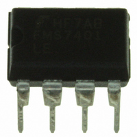
FMS7401LEN Fairchild Semiconductor, FMS7401LEN Datasheet - Page 40

FMS7401LEN
Manufacturer Part Number
FMS7401LEN
Description
IC CTRLR POWER DGTL EEPROM 8DIP
Manufacturer
Fairchild Semiconductor
Datasheet
1.FMS7401LVN.pdf
(81 pages)
Specifications of FMS7401LEN
Applications
Digital Power Controller
Core Processor
8-Bit
Program Memory Type
EEPROM (1 kB)
Ram Size
64 x 8
Number Of I /o
6
Voltage - Supply
2.7 V ~ 3.6 V
Operating Temperature
-40°C ~ 85°C
Mounting Type
Through Hole
Package / Case
8-DIP (0.300", 7.62mm)
Mounting Style
Through Hole
Lead Free Status / RoHS Status
Lead free / RoHS Compliant
Interface
-
Controller Series
-
Lead Free Status / Rohs Status
Lead free / RoHS Compliant
Other names
FMS7401LEN_NL
FMS7401LEN_NL
FMS7401LEN_NL
Available stocks
Company
Part Number
Manufacturer
Quantity
Price
Company:
Part Number:
FMS7401LEN14
Manufacturer:
Rohm
Quantity:
21 626
FMS7401L
6.3
When the PWM Timer 1 circuit is configured in Input Capture Mode, the T1HS2 signal is used as an input of the Timer 1
circuit instead of an output as in PWM Mode. The G5/T1HS2 device pin should be configured by software as an input port.
The Timer 1 circuit may be programmed to capture the TMR1 counter value in the T1RA register with every rising or falling
edge transition of the T1HS2 input. With each TMR1 capture, the T1PND bit of the T1CNTRL register is set. For synchroniza-
tion purposes, the T1HS2 input is synchronized with the F
imum of three F
Once the Timer 1 circuit is configured for Input Capture Mode, the TMR1 counter starts incrementing continuously from
0x000 through 0xFFF until the Timer 1 is returned to a disabled PWM operating mode. Once the TMR1 counter overflows
(transitions from 0xFFF to 0x000) the T1C0 pending bit on through T1CNTRL register is set.
In Input Capture Mode, it is still possible to generate output signals with variable duty-cycle thanks to the T1CMPA and
T1CMPB compare registers. If enabled, the T1HS1 and ADSTROBE output signals may be generated as in PWM Mode. Refer
to the previous
1. Refer to
2. Refer to the
3. The PLL’s (F
4. Refer to the
5. The three PS bits have no affect on the dead time, only the TMR1 counter.
6. Hardware interrupts are not executed by the microcontroller core unless the Global Interrupt enable (G) flag of the Status register is set. Refer to the
7. The Timer 1 hardware interrupt will be executed in the defined priority order. Refer to the
8. The full bridge requires two additional output ports to complete the bridge configuration.
9. Refer to the
10.Refer to the
40
controller Core
G5/T1HS2
F
Input Capture Mode
T1CLK
Table 30
Electrical Characteristics
ADC Circuit
I/O Ports
(FS=0)
Device Memory
section of the datasheet for details.
Pulse Width Modulation (PWM) Mode
) output is not affected by the FS[1:0] bit value of the PSCALE register and merely shares the FS[1:0]=00 divide factor.
of the
T1CLK
T1C2
Fin
section of the datasheet for additional details.
Control
Device Memory
section of the datasheet for additional details.
Edge
PS2 PS1 PS0
DIVIDER
PSCALE
cycle TMR1 capture delay will occur with each edge transition on the G5/T1HS2 device pin.
CLOCK
section of the datasheet for details regarding the initialization registers.
Fout
section of the datasheet.
section of the datasheet for the detailed memory map.
Figure 13. Timer 1’s Input Capture Mode Block Diagram
T1CMPB
[11:0]
12
12
TMR1
[11:0]
T1RA
[11:0]
T1CMPA
section of the datasheet for details.
[11:0]
T1CLK
T1PND
T1C0
clock before being allowed to trigger a TMR1 capture. A max-
TMR1=T1CMPA
8-Bit Microcontroller Core
TMR1=T1CMPB
T1BOUT
ENDAS
PORTGD
1
section of the datasheet for details.
0
PRODUCT SPECIFICATION
ADSTROBE
REV. 1.0.3 1/24/05
8-Bit Micro-
G1/AIN3
G0/T1HS1


