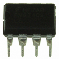
FMS7401LEN Fairchild Semiconductor, FMS7401LEN Datasheet - Page 31

FMS7401LEN
Manufacturer Part Number
FMS7401LEN
Description
IC CTRLR POWER DGTL EEPROM 8DIP
Manufacturer
Fairchild Semiconductor
Datasheet
1.FMS7401LVN.pdf
(81 pages)
Specifications of FMS7401LEN
Applications
Digital Power Controller
Core Processor
8-Bit
Program Memory Type
EEPROM (1 kB)
Ram Size
64 x 8
Number Of I /o
6
Voltage - Supply
2.7 V ~ 3.6 V
Operating Temperature
-40°C ~ 85°C
Mounting Type
Through Hole
Package / Case
8-DIP (0.300", 7.62mm)
Mounting Style
Through Hole
Lead Free Status / RoHS Status
Lead free / RoHS Compliant
Interface
-
Controller Series
-
Lead Free Status / Rohs Status
Lead free / RoHS Compliant
Other names
FMS7401LEN_NL
FMS7401LEN_NL
FMS7401LEN_NL
Available stocks
Company
Part Number
Manufacturer
Quantity
Price
Company:
Part Number:
FMS7401LEN14
Manufacturer:
Rohm
Quantity:
21 626
Table 11. Digital Delay (DDELAY) Register Bit Definitions
1. Refer to the
2. Refer to the
3. Hardware interrupts are not executed by the microcontroller core unless the Global Interrupt enable (G) flag of the Status register is set. Refer to the
4. Refer to the
REV. 1.0.3 1/24/05
PRODUCT SPECIFICATION
Bit
COMPEN
PWMINT
EPWM
OFFMODE
DD[3:0]
Microcontroller Core
COMPEN
Bit 7
ADC Circuit
I/O Ports
Clock Circuit
Description
(0) Disable the Programmable Comparator circuit.
(1) Enable the Programmable Comparator circuit.
(0) The input of the G6 MIW circuit network is the G6/-A
(1) The input of the G6 MIW circuit network is the PWMOFF output signal (not the G6/-A
(0) Enables the Digital Delay Filter circuit. The PWMOFF output is triggered by C
(1) Disables the Digital Delay Filter circuit and the PWMOFF output signal.
(0) PWM outputs switched off and Timer 1 stops after a comparator detection with delay.
(1) PWM outputs switched off for the current PWM cycle only.
Digital delay after C
section of the datasheet for details.
section of the datasheet for details.
PWMINT
section of the datasheet for additional details.
Bit 6
section of the datasheet for details regarding the F
OUT
EPWM
Bit 5
triggers high, T
Comparator
PWMOFF
Figure 10. Digital Delay Timing
T1HS1
T1HS2
Output
Digital
Delay
DDELAY Register (addr. 0xA2)
OFFMODE
DDELAY
Bit 4
Start
= DD • (1/F
RCLK2
T
DDELAY
clock.
IN
RCLK2
device pin.
Bit 3
)
Sample
Bit 2
OUT
DD[3:0]
after the programmed delay (T
IN
device pin).
Bit 1
Bit 0
FMS7401L
8-Bit
DDELAY
31
).


