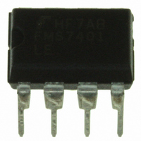
FMS7401LEN Fairchild Semiconductor, FMS7401LEN Datasheet - Page 3

FMS7401LEN
Manufacturer Part Number
FMS7401LEN
Description
IC CTRLR POWER DGTL EEPROM 8DIP
Manufacturer
Fairchild Semiconductor
Datasheet
1.FMS7401LVN.pdf
(81 pages)
Specifications of FMS7401LEN
Applications
Digital Power Controller
Core Processor
8-Bit
Program Memory Type
EEPROM (1 kB)
Ram Size
64 x 8
Number Of I /o
6
Voltage - Supply
2.7 V ~ 3.6 V
Operating Temperature
-40°C ~ 85°C
Mounting Type
Through Hole
Package / Case
8-DIP (0.300", 7.62mm)
Mounting Style
Through Hole
Lead Free Status / RoHS Status
Lead free / RoHS Compliant
Interface
-
Controller Series
-
Lead Free Status / Rohs Status
Lead free / RoHS Compliant
Other names
FMS7401LEN_NL
FMS7401LEN_NL
FMS7401LEN_NL
Available stocks
Company
Part Number
Manufacturer
Quantity
Price
Company:
Part Number:
FMS7401LEN14
Manufacturer:
Rohm
Quantity:
21 626
FMS7401L Pin Definitions
REV. 1.0.3 1/24/05
PRODUCT SPECIFICATION
SOIC
PDIP
1
2
3
4
5
6
7
8
–
–
–
–
–
–
8-Pin
Pin Number
TSSOP
3
4
5
6
7
8
1
2
–
–
–
–
–
–
TSSOP
14-Pin
SOIC
PDIP
10
12
14
11
13
1
3
6
7
9
2
4
5
8
ADSTROBE
Pin Name
G1/AIN3/
SR_GND
G7/AIN4/
NC/GND
G4/AIN0
G2/AIN2
G3/AIN1
NC/VCC
G6/-A
RESET
T1HS1
T1HS2
GND
VCC
A
G0/
G5/
OUT
IN
General purpose I/O port (bit 4 of the I/O configuration registers).
AIN0 analog input of the ADC (autozero amplifier’s positive terminal).
Programmable Comparator non-inverting input, if COMPSEL=0.
Digital ground pin.
General purpose I/O port (bit 2 of the I/O configuration registers).
AIN2 analog input of the ADC.
Programmable Comparator non-inverting input, if COMPSEL=1.
General purpose I/O port (bit 1 of the I/O configuration registers).
AIN3 analog input of the ADC.
External digital clock input.
PWM Timer 1’s ADSTROBE output.
General purpose I/O port (bit 3 of the I/O configuration registers).
AIN1 analog input of the ADC.
Internal current source generator pin.
General purpose I/O port (bit 0 of the I/O configuration registers).
PWM Timer 1’s T1HS1 output.
General purpose I/O port (bit 5 of the I/O configuration registers).
PWM Timer 1’s T1HS2 output.
Supply voltage input.
AIN0 analog input of the ADC (autozero amplifier’s negative terminal). SR_GND is
internally connected to GND in the 8-pin FMS7401L.
General purpose I/O port (bit 6 of the I/O configuration registers).
Uncommitted amplifier negative analog input.
General purpose I/O port (bit 7 of the I/O configuration registers).
AIN4 analog input of the ADC.
Uncommitted amplifier analog output.
In the FMS7401L, pin 8 is internally connected to GND. Externally, pin 8 should be left
unconnected or connected to GND.
Active low external reset input.
In the FMS7401L, VCC is internally connected to pin 13. Externally, pin 13 should either
be left unconnected or connected to pin 13.
Pin Function Description
FMS7401L
3


